
The role of substrate purity and its crystallographic orientation in the defect density of chemical vapor deposition grown monolayer graphene†
Munu Borahab,
Dilip K. Singha,
Kiran M. Subhedara and
Sanjay R. Dhakate*ab
aPhysics and Engineering of Carbon, Division of Material Physics and Engineering, CSIR-National Physical Laboratory, New Delhi-110012, India. E-mail: dhakate@mail.nplindia.org; Tel: +91-11-4560-9388
bAcademy of Scientific & Innovative Research (AcSIR), CSIR-NPL Campus, New Delhi-110012, India
First published on 3rd August 2015
Abstract
Defect free mono-layer graphene sheet growth has remained a challenge towards its huge potential applications in electronic and photonic devices. Here, we are reporting about the role of the copper substrate purity and its crystallographic orientation in the quality of the graphene grown using a low pressure chemical vapor deposition technique. Graphene is grown on three different (Cu-I, Cu-II and Cu-III) substrates of different purity under analogous conditions of optimized pre-growth annealing and cleaning processes. Irrespective of the purity level of all the substrates, it is demonstrated that monolayer graphene (IG′/IG ∼ 4) with different defect density is observed. The amount of defects and the defect density in the three samples is correlated with the different lattice planes of Cu, which are participating during the growth process. The size of the lattice grain advance upon annealing is observed and it is substrate purity dependent. This reveals that graphene growth is favored by either the (111) or the (100) plane or both. It is demonstrated that the substrate purity is extremely accountable for the growth of defect free monolayer graphene for device applications which require ballistic transport properties.
Introduction
The synthesis of large area defect free graphene for device fabrication suggests that the key to controlling the growth parameter still remains unknown and uncontrolled.1–4 In spite of a number of attempts to reveal the parameters of defect free graphene growth, a consensus about defect free graphene growth has not been reached so far, with graphene having theoretically predicted transport properties. Graphene is predicted to show relativistic transport properties with an electron mobility as high as 200![[thin space (1/6-em)]](https://www.rsc.org/images/entities/char_2009.gif) 000 cm2 V−1 s−1 (ref. 5) with the ability to sustain a very high current density (a million times higher than that of copper)6 and electrical conductivity 2 × 10³ S cm−1 (ref. 7) with zero effective mass.8 Whereas in contrast to theoretical predictions, experiments show widely varying values of carrier mobility of ∼4000–8000 cm2 V−1 s−1 which is roughly three orders of magnitude lower than the theoretical predictions.6–8 A number of techniques have been attempted to grow graphene like mechanical exfoliation of graphite,9 epitaxial growth on SiC,10 chemical reduction of exfoliated graphene oxide11 and chemical vapor deposition (CVD).12 Li and colleagues for the first time demonstrated CVD based growth in 2009.13 CVD based graphene growth is cost effective and can be used to grow large size sheets12 while mechanical exfoliation is a time consuming process and mostly gives small size graphene sheets. SiC based growth is a commercially nonviable technique. To date the best possible mobility in the case of CVD based graphene is on average ∼3000 cm2 V−1 s−1 (ref. 14) while the other two techniques show much higher values of electron mobility ∼5000 (ref. 15) and ∼6450 cm2 V−1 s−1.16 Currently dendritic growth, the formation of multilayers, and the lower carrier mobility are issues of concern among researchers working with CVD based graphene growth.17,18 Attempts have been made by growing graphene on various transition metals and their alloys,19,20 on P-block elements (Ga), using a liquid Cu surface21,22 and on copper substrates with chromium oxide coatings.23
000 cm2 V−1 s−1 (ref. 5) with the ability to sustain a very high current density (a million times higher than that of copper)6 and electrical conductivity 2 × 10³ S cm−1 (ref. 7) with zero effective mass.8 Whereas in contrast to theoretical predictions, experiments show widely varying values of carrier mobility of ∼4000–8000 cm2 V−1 s−1 which is roughly three orders of magnitude lower than the theoretical predictions.6–8 A number of techniques have been attempted to grow graphene like mechanical exfoliation of graphite,9 epitaxial growth on SiC,10 chemical reduction of exfoliated graphene oxide11 and chemical vapor deposition (CVD).12 Li and colleagues for the first time demonstrated CVD based growth in 2009.13 CVD based graphene growth is cost effective and can be used to grow large size sheets12 while mechanical exfoliation is a time consuming process and mostly gives small size graphene sheets. SiC based growth is a commercially nonviable technique. To date the best possible mobility in the case of CVD based graphene is on average ∼3000 cm2 V−1 s−1 (ref. 14) while the other two techniques show much higher values of electron mobility ∼5000 (ref. 15) and ∼6450 cm2 V−1 s−1.16 Currently dendritic growth, the formation of multilayers, and the lower carrier mobility are issues of concern among researchers working with CVD based graphene growth.17,18 Attempts have been made by growing graphene on various transition metals and their alloys,19,20 on P-block elements (Ga), using a liquid Cu surface21,22 and on copper substrates with chromium oxide coatings.23
A number of physical parameters like gas flow rates, the nature of the substrate and thermodynamic parameters are expected to play crucial roles in the quality of the graphene grown.24 In recent studies, the effect of the substrate on the growth rate and uniformity of graphene has been primarily addressed. In the case of the polycrystalline copper substrate, more favorable growth has been observed from the Cu(111) plane than that from Cu(100) for uniform monolayer graphene synthesis.25 In contrast to this, Rasool et al.26 have reported that the quality of graphene is controlled by the active sites of nucleation rather than the atomic structure of the copper substrate, also (100) was established as more preferential. Whereas Wood et al. (2011) studied the growth through Electron Back Scattering Diffraction (EBSD) and observed perfect graphene sheet growth in the Cu(111) plane compared to that of Cu(100).27 Although the growth of defect free graphene over Cu substrates with different crystallographic orientation in the Cu(100) or Cu(111) plane is largely debated, the role of the substrate purity and the evolution of various crystallographic orientations during the pre-growth annealing process has not been experimentally explored in a broad sense. Vlassiouk et al.28 have studied the morphology and size of graphene domains with varying partial pressures of CH4 and H2. They have performed their experiment using two different Cu substrates namely low (99.8%, Alfa Aesar) and high (99.999%, Alfa Aesar) respectively. Similarly Liu et al.29 also have concluded from their work on monolayer graphene synthesis by CVD, that the partial pressure of hydrocarbons and the purity of the copper substrate play an important role in determining the uniformity of the graphene layers grown by CVD. It is necessary to address the issues of controlled growth like the nucleation density, the surface adsorption mechanism of carbon atoms over the substrate, the crystallinity and the purity of the substrate used.30 Additionally various factors during post growth transfer processes also affect the quality of graphene in terms of its sheet resistance and charge mobility, like cracks and wrinkles which originate along the grain boundaries during the transfer process.31 In this paper, we report about the role of substrate purity and its crystallographic orientation towards the quality of the graphene grown.
Experimental section
Graphene sheets were grown on three types of Cu, namely Cu-I, Cu-II and Cu-III with purity and thickness 99% (50 μm), 99.8% (25 μm) and 99.999% (25 μm) pure procured from Klim and Alfa Aesar respectively. The impurities present in the copper include different concentrations of Al, K, Si, C, Li, Ti, Fe, Na, I and S as specified by the supplier. The gases argon (Ar), hydrogen (H2) and methane (CH4) of 99.9% purity were used for growth. Acetone (99.5% purity), isopropyl alcohol (IPA 99.7% purity), acetic acid (99.8% purity), poly-methyl methacrylate (PMMA), chlorobenzene (99% purity) and ammonium persulfate (98% purity) were obtained from Sigma-Aldrich.Copper substrate cleaning
Cu foils were kept in acetone and ultrasonicated for 1 minute and air dried under a flow of nitrogen. Further, it was sonicated in isopropyl alcohol for 1 min and again air dried. After cleaning, the copper foils were soaked in acetic acid and mildly sonicated for 10 minutes at low frequency. High frequency sonication was purposely avoided to stop the formation of a non-uniform wrinkled surface. After sonication it was washed repeatedly with deionized water. Finally, the foils were again cleaned with IPA and allowed to air dry under a flow of nitrogen.Graphene growth in CVD
Graphene sheets were synthesized using a single zone tubular split furnace with a horizontal quartz reactor of length 1.25 m and with an internal diameter of 80 mm, schematically shown in Fig. S1 (ESI†). The gas flow rate was controlled using electronic mass flow controllers AALBORG, USA.All three different Cu foils were placed on the quartz substrate and kept in the central isothermal zone of the furnace which was heated up to 1000 °C in a H2 and Ar gas atmosphere at flow rates of 4 sccm and 15 sccm respectively (total pressure 0.135 torr) into the system. The foils were annealed for 30 min to remove residual oxide so as to smooth the surface for the growth and subsequently CH4 gas was introduced as a carbon precursor at a flow rate of 25 sccm for 10 min, in the presence of H2 (total pressure 0.29 torr). After growth, samples were cooled to room temperature at a cooling rate of 25 °C min−1 under an Ar and H2 atmosphere see ESI (Fig. S1†). The growth was attempted on a number of substrates before arriving to the conclusions.
Transfer process of graphene
The PMMA solution was prepared by dissolving 4.6 g of PMMA in 100 ml chlorobenzene which was coated on the graphene films using a spin coater (Spin NXG-P1, Apex Equipment). The PMMA coated sample was kept on a hot plate for 1 min at 180 °C for baking. To etch the Cu from graphene, the PMMA coated graphene film was kept in an aqueous solution of 20 g of ammonium persulfate (H8N2O8S2) in deionized water. After complete etching of Cu within 8–10 hours, the resultant sample was transferred onto the final silicon substrate followed by soaking in an acetone solution for the removal of the polymer coating from the graphene sheet.Characterization
Optical microscopy (Zeiss Axiolab A1) was performed to study the evolution of grain boundaries on the copper substrates before and after annealing as well as on the graphene grown substrate. The Raman spectra of graphene were taken using a Renishaw spectrophotometer (micro-Raman model inVia Reflex) with 514 nm laser excitation. For the Raman spectra a 50× (NA 0.75) objective was used with a laser power of 5 mW (laser spot size ∼ 0.8 μm).The crystal structures of the copper foil before and after annealing and the graphene–copper samples were studied with X-ray diffraction (XRD, D-8 Advanced Bruker diffractometer) using CuKα radiation (λ = 1.5418 Å).
The surface morphology of the as grown graphene on the copper substrates was observed using a scanning electron microscope with back scattering mode (SEM, VP-EVO, MA-10, Carl-Zeiss, UK) operating at an accelerating potential of 10.0 kV.
Results and discussions
Fig. 1(a)–(c) show the typical optical micrographs of three different copper foils (Cu-I, Cu-II, Cu-III) of different purity after cleaning. The bare copper foils consist of different orientations of grains on the surface (appearing as parallel lines in the optical micrographs), see Fig. 1(a–c). These grains on the surface arise from the processing and are also due to the difference in the purity of copper. The initial orientation of grains and internal stress within the foil are expected to influence the evolution of the grain size and orientation during annealing.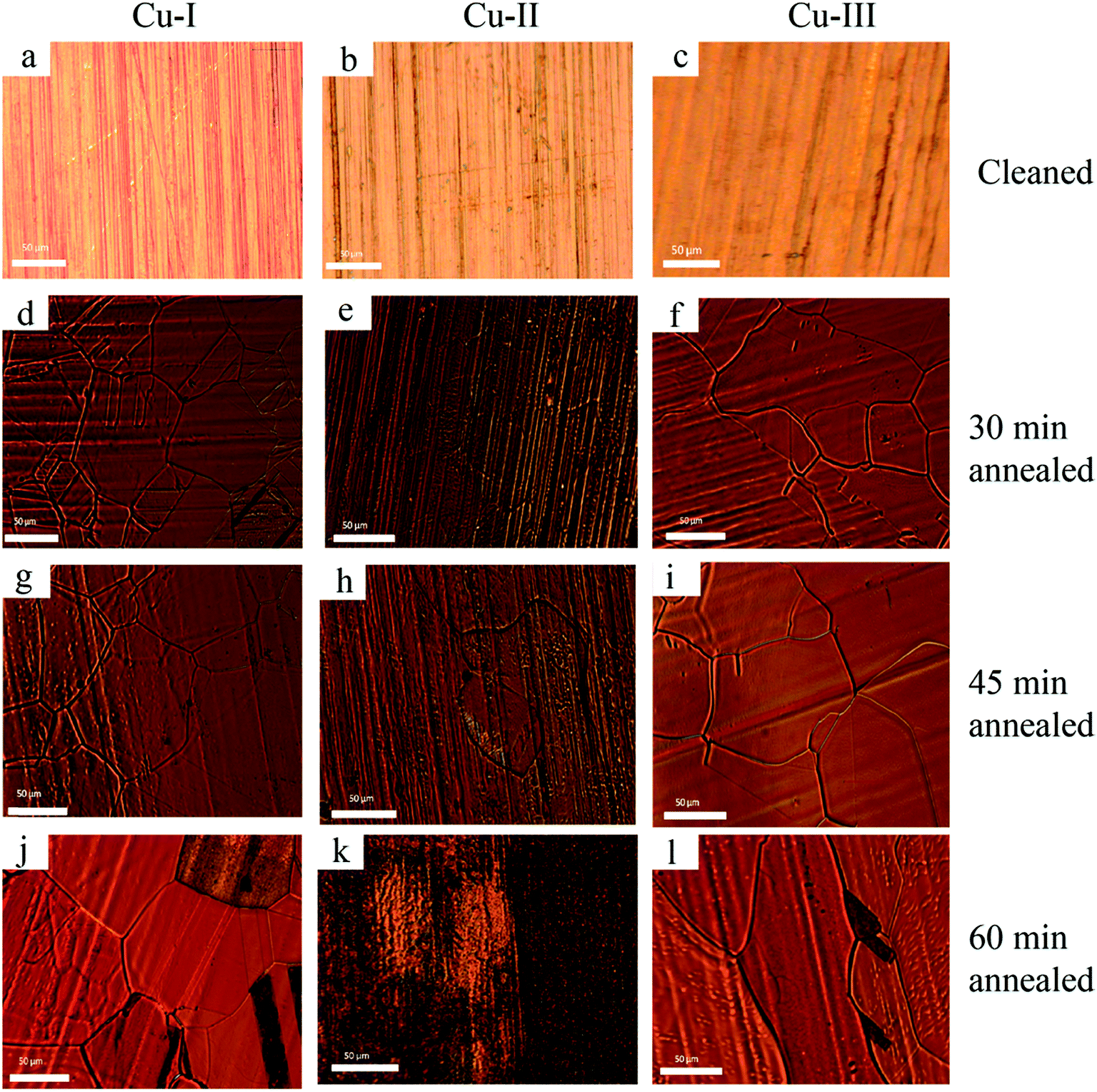 | ||
| Fig. 1 Optical micrographs of the copper substrates after annealing at 1000 °C for 30 min, 45 min, and 60 min respectively. Cu-I (a, d, g and j), Cu-II (b, e, h and k) and Cu-III (c, f, i and l). | ||
The copper substrates were chemically cleaned and subsequently annealed at 1000 °C under a flow of a mixture of Ar and H2 gas (4:1) to remove the native oxide layer and smoothen the surface. The substrates were annealed for 30 min, 45 min and 60 min to monitor the evolution of randomly curved grain boundaries as shown in Fig. 1(d–l). Fig. 1(d) shows the co-existence of large and small grains in Cu-I (i.e. twin formation). This indicates the occurrence of secondary grain growth in Cu-I upon annealing. Fig. 1(d) and (f) show defined regions of grain boundary formation for Cu-I and Cu-III annealed for different periods, while Cu-II shows the formation of elongated open grain boundaries, Fig. 1(e). A single large twin forms and grows upon annealing so that a portion of the original boundary is replaced by an immobile coherent twin boundary and a mobile incoherent boundary when the surface energy considerations are favorable resulting in large size grain growth in the case of Cu-I and Cu-III upon annealing. While in the case of Cu-II, upon annealing the formation of open ended long grain boundaries occurs due to unfavorable surface energy considerations.32 It is clear that the substrate with higher purity i.e. Cu-III shows larger size grain growth after annealing for 30 min, 45 min and 60 min as shown in Fig. 1(f), (i) and (l) respectively compared to Cu-I and Cu-II. With the increase of annealing time from 30 minutes to 45 minutes, the size of the grain boundaries increases. While a further increase in the annealing period to 60 minutes, leads to the formation of ripples and regions of increased surface roughness which appear as dark patches as observed with an optical microscope (see Fig. 1(j) and (l)). The 30 min annealing was found to be the most suitable condition of pre-growth annealing from the X-ray diffraction studies shown in Fig. S1 (ESI†). Although the grain size increases with increasing annealing time from 30 min to 60 min, the preferred planes of growth (111) and (100) show monotonically decreasing intensity in the X-ray diffraction pattern along with surface degradation in terms of roughness. Optically the substrate with low purity Cu-I shows relatively less change in surface roughness as compared to Cu-II and Cu-III upon 60 min of annealing. This is due to the higher melting temperature for the substrates with higher impurity (i.e. Cu-metal alloys) and is also due to the high thickness of the substrate Cu-I as compared to Cu-II and Cu-III.
Fig. 2 shows the optical images (Fig. 2(a–c)) and SEM micrographs (Fig. 2(d–f)) of graphene grown for 10 min on the Cu substrates. The substrates were annealed at 1000 °C for 30 min before growth. During growth, the curvature of the grain boundaries on the Cu substrates increases the adsorption energy of incoming carbon atoms and acts as nucleation sites, helping the formation of longer strip like graphene.33 In Fig. 2(a) and (c), the optical images demonstrate the restricted growth within the closed regions of the grain boundaries which is apparent from the restricted regions of similar contrast.
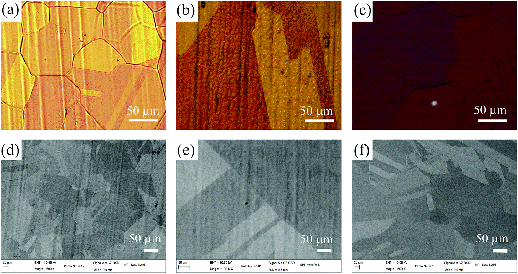 | ||
| Fig. 2 Optical microscopy images of graphene grown on the copper substrates (a) Cu-I, (b) Cu-II and (c) Cu-III. SEM-back scattering images of graphene on (d) Cu-I, (e) Cu-II and (f) Cu-III grown by LPCVD at 1000 °C. | ||
Fig. 2(d)–(f) show the SEM backscattering images of graphene grown for 10 min on the annealed copper substrates. The metallic substrate Cu is expected to show relatively stronger elastic backscattering of electrons and hence it appears as a light contrast compared to the grown graphene. Fig. 3(a)–(c) show the optical micrographs of transferred graphene on a SiO2/Si substrate grown on Cu-substrates of different purity Cu-I, Cu-II and Cu-III respectively. The approximate area of the continuous graphene film synthesized using three different substrates are Cu-I ∼ 0.926, Cu-II ∼ 0.718 and Cu-III ∼ 0.569 mm2 in Fig. 3(a)–(c). Graphene transferred from Cu-I shows relatively larger regions of folded and agglomerated morphology as compared to the graphene transferred from Cu-II and Cu-III, see Fig. 3(a)–(c). Fig. 3(d) shows the Raman spectra of the transferred graphene sheets from the three substrates of different purity. The Raman spectra show three prominent features at ∼1347, 1584 and at ∼2685 cm−1 known as the D-band, G-band and G′-band respectively.
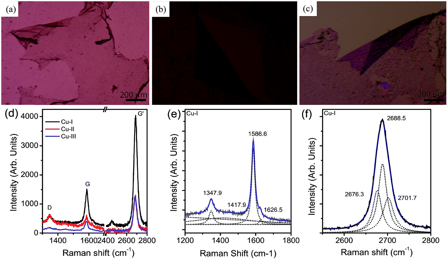 | ||
| Fig. 3 Optical images of the transferred graphene sheet on a SiO2/Si substrate, which was grown on (a) Cu-I, (b) Cu-II and (c) Cu-III. (d) Raman spectra of the transferred graphene on a SiO2/Si substrate that was synthesized on three Cu substrates of different purity. (e) Lorentzian fit for the D and G peaks of Cu-I graphene and (f) Lorentzian fit for the G′ peak of Cu-I graphene. | ||
These spectra were fitted with Lorentzian line shape and the corresponding spectra information related to all the three types of graphene is enlisted in Table 1. A typical fitting for the sample transferred from the Cu-I substrate (referred to as Cu-I graphene) is shown in Fig. 3(e) for the D and G peaks and in Fig. 3(f) for the G′-band separately for clarity. Cu-I and Cu-II show a D-band at ∼1347 cm−1 with FWHM of ∼31 cm−1. While Cu-III graphene shows a D-band at 1345 cm−1 with an almost double peak-width. Cu-II graphene shows the highest peak intensity of the D-band with 295 counts while the Cu-I graphene shows 206 counts and the Cu-III graphene shows the lowest intensity of 81 counts. The difference in the peak width of Cu-III possibly arises due to the presence of more disordered carbon in the Cu-III surface with the lowest density, while Cu-I and Cu-II contain localized defects. The G-band position shifts monotonically from 1586.6 to 1584.9 and 1582.9 cm−1 i.e., towards a lower Raman shift with increasing Cu purity. This indicates higher strain in the grown graphene with increasing purity of the Cu substrate.
| Sample | D peak position (cm−1) | G peak position (cm−1) | G′ peak position (cm−1) | G′-FWHM (cm−1) | IG′/IG | ID/IG |
|---|---|---|---|---|---|---|
| Cu-I | 1347 | 1586 | 2688 | 23.5 | 3.7 | 0.2 |
| Cu-II | 1347 | 1584 | 2685 | 21.2 | 3.9 | 0.9 |
| Cu-III | 1345 | 1582 | 2683 | 24.4 | 3.5 | 0.3 |
The G-band shows nearly the same peak width in the case of graphene grown on the Cu-I and Cu-III substrates of nearly 22 cm−1, while Cu-II graphene shows a peak width of about 28 cm−1. The higher peak width observed in the case of Cu-II graphene is in agreement with the higher D-band intensity observed for it, indicating the presence of the highest defect density compared to the other two samples Cu-I and Cu-III. The second order G′ mode shows a nearly fourfold higher intensity compared to the first-order graphitic G peak for all the three samples as expected from the single layered graphene structure.34 In the case of graphene, an intense second order G′ mode arises due to inter-valley double resonance Raman scattering.35–37 Fitting with Lorentzian line shape shows three components of the G′ peak as observed earlier by Dresselhaus et al. The three peak structure arises due to a two photon assisted second order Raman scattering process.38 In the two photon inter-valley scattering process two high symmetry points K and K′ of the first Brillouin zone of the graphene participate. Out of four possible phonon assisted transitions between the valence band and the conduction band two are degenerate resulting in a three peak structure of the G′-band.38 The G′-band shows blue-shift with increasing purity of the Cu substrate. Graphene grown on Cu-I foil (low purity 99%) shows a G′ peak at 2688 cm−1, grown on Cu-II at 2685 cm−1 and grown on Cu-III at 2683 cm−1. The observed shift in the G′ peak position with the purity of the copper substrate is in agreement with the shifts registered for the G-band. The quality of the graphene grown is usually expressed in terms of the IG′/IG intensity ratio while ID/IG (the defect ratio) and FWHM of G′ give information about the number of layers and the defect intensity present in graphene.34,39 The electronic band structure around the Fermi level of multilayer graphene plays an important role in inter-valley double resonance Raman.35 The three samples Cu-I graphene, Cu-II graphene and C-III graphene show similar IG′/IG ratios of 3.7, 3.9 and 3.5 with varying ID/IG ratios of 0.2, 0.9 and 0.3 respectively. The ratio of IG′/IG is highest in the case of graphene grown on the Cu-II substrate compared to Cu-I and Cu-III. The ID/IG ratio of defect density in the synthesized graphene is highest in the case of the graphene grown on Cu-II. This indicates that Cu-II favors highly crystalline graphene with relatively more localized defects. We have also measured the defect density (nD) from the Raman intensity profile using empirical relations presented by Cançado et al.40
| nD (μm−2) = (1.8 ± 0.5)/λL4 × 1014(ID/IG) |
The average defect density of graphene grown on the Cu-I, Cu-II and Cu-III substrates was found to be 515.76, 2320.93 and 773.64 μm−2 respectively. Defect density (nD) is inversely proportional to the square of the inter-defect distance41 and the corresponding ID/IG for a specific inter-defect distance (LD), depends on the laser energy.40,42 Defect density estimates the limit of graphene mobility. The defect density present is correlated with the crystal plane of the substrate used for graphene growth. For instance graphene grown on the Cu-II substrate possesses the highest defect density in comparison to the other substrates, Cu-I and Cu-III. This may be due to the presence of a specific crystallographic plane participating in the graphene growth as discussed in the XRD analysis in a subsequent section.
Further, the observations are validated by Raman spectroscopy analysis at various locations over the samples as shown in Fig. 4. Fig. 4(a)–(c) show the optical micrographs and marked points at which the spectra was recorded for the Cu-I graphene, Cu-II graphene and Cu-III graphene sheets. The corresponding spectra are depicted in Fig. 4(d)–(f) for Cu-I graphene, Cu-II graphene and Cu-III graphene, numbered sequentially as the spot positions. They reveal monolayer graphene growth with discontinuity as reflected by various regions with a ratio IG′/IG > 3 and equally many other points showing the absence of characteristic features. Fig. 4(e) and (f) show Raman spectra taken over various points for Cu-II and Cu-III graphene. The Raman spectra measured over unfolded regions confirm the growth of single layer graphene (IG′/IG ≈ 3)43,44 whereas, in folded regions the IG′/IG ratio is <2. Additionally, in the folded regions the G′ and G peaks appear at different Raman shifts, due to their similarity in behavior with bi-layer or few layer graphene.45 Similarly, the ID/IG ratio is different in the case of the folded and unfolded regions. It is nearly double in the case of the folded regions compared to the unfolded regions. One of the possible sources of high D-band intensity in the case of the folded regions is the deformation of the 2D graphene structure due to left out residual PMMA during the transfer process. The Raman spectroscopic measurements at various points of Cu-III graphene shows that it has a high crystallinity monolayer structure (max. IG′/IG = 4.24) with a very low defect density even in folded regions (Fig. 4(f)).
 | ||
| Fig. 4 Optical micrographs of transferred graphene with different marked positions (a) Cu-I graphene, (b) Cu-II graphene and (c) Cu-III graphene. (d)–(f) Corresponding Raman spectra as marked in (a), (b) and (c) respectively. | ||
To understand the difference in the crystallinity and defect density of the graphene grown over three substrates with varying purity, we probed the role of substrate crystallinity, its surface planes and its evolution during annealing and growth using XRD. Fig. 5(a) shows the XRD patterns of the cleaned substrates Cu-I, Cu-II and Cu-III recorded using Bragg–Bento geometry and a Cu Kα1 line. The cleaned Cu-I and Cu-II substrates show peaks corresponding to (111), (100), (110), (311) and (400), while Cu-III shows peaks corresponding to (111), (100) and (311). Peaks corresponding to (110) and (400) were not observed in case of the Cu-III substrate. In the case of Cu-I and Cu-II the peak corresponding to the (100) lattice plane shows the highest intensity while in case of Cu-III, the peak corresponding to the (111) lattice facet shows the highest intensity. Fig. 5(b) shows the XRD pattern of the Cu-I substrate after cleaning (black curve), after annealing at 1000 °C for 30 min (red curve) and after growth for 10 min (blue curve). The relative peak intensity of the (111) and (100) peaks changes significantly upon annealing for 30 minutes before growth. In the case of the cleaned Cu-I substrate the (100) peak has the highest peak intensity while upon annealing the (111) peak becomes more intense than the (100) peak.
 | ||
| Fig. 5 X-ray diffraction patterns of the copper substrates after cleaning, annealed and after growth. (a) Cleaned copper substrate of the three copper foils, (b) Cu-I, (c) Cu-II and (d) Cu-III. | ||
This shows that in Cu-I after annealing at 1000 °C for 30 minutes (at low pressure < 100 mtorr), the preferred crystal plane for growth is (111). The peak intensity of the (100), (110), (311) and (400) planes are suppressed upon annealing. The relative change in the peak intensity of various planes occurs due to the high degree of mobility of the copper atoms at an elevated temperature of 1000 °C (i.e. only 83 °C less than the Cu melting point) leading to the merging of facets. The XRD spectrum of the Cu-I graphene sample (i.e., after 10 min growth on the annealed substrate at a pressure of 0.29 torr) shows splitting of the (111) peak into multiple components. This represents the varying percentage of compressive strain along the (111) plane and is the most favored plane for growth among all others.26 Reflections from the lattice planes (100) and (311) also show a shift to higher Bragg angles upon growth, representing compressive strain along these planes as well.
Fig. 5(c) shows the XRD pattern of Cu-II after cleaning (black curve), after annealing (red curve) and after graphene growth (blue curve). In the case of Cu-II the (100) facet is the most prominent before annealing, analogous to Cu-I. In addition to this, the cleaned Cu-II substrate consists of the (111), (110), (311) and (400) planes. After annealing Cu-II, only the (100) plane is observed and reflections from (111), (110) and (400) are of negligible intensity. The (100) peak shifted to a lower Bragg angle upon annealing and it shows multiple splitting after growth and shifts to a higher Bragg angle. In addition to the (100) peak, (400) appears with weak intensity after growth. Although the cleaned Cu-I and Cu-II substrates initially showed similar diffraction patterns i.e. (111), (100) (110), (311) and (400) after annealing, depending upon the substrate purity level they behave differently.
Fig. 5(d) shows the XRD pattern of Cu-III after cleaning, after annealing and after graphene growth. The cleaned Cu-III substrate consists of peaks at 2θ values of 53.45, 77.00 and at 92.90° which are located at different positions than the peaks observed in the case of Cu-I and Cu-II. These peaks are close to the assigned peaks of the (100), (110) and (311) planes observed in the case of Cu-I and Cu-II. Peaks at 2θ values of 53.45, 77.00 and 92.90° are located at higher Bragg angles than the expected peaks at 2θ = 50.33, 74.20 and 89.90° corresponding to the (100), (110) and (311) planes indicating the presence of compressive strain along these planes. After the annealing peak corresponding to the (111) plane shows maximum intensity while the (100) and (311) planes shift towards lower Bragg angles at the expected peak values similar to Cu-I and Cu-II. After growth, the XRD pattern of Cu-III shows reflections of the (100) and (311) planes. The (111) plane shows negligibly small intensity after growth, although it had been prominent after annealing. This makes it difficult to comment on whether the (111) plane participates during growth or not. After growth, the (100) plane shows splitting of the peak indicating its large participation in graphene growth. The behavior of Cu-III is analogous to Cu-II where growth is from the (100) lattice plane, while it differs from Cu-I where it occurs from the (111) plane. This indicates that as the purity of the substrate used increases the growth begins to favor the (100) lattice plane relative to the (111) plane.
The XRD line profile of Cu-I shows that it contains a large number of different facet steps and grain boundaries having high activation energy for hydrocarbon decomposition that act as graphene nucleation sites.35 Due to these characteristics in the case of Cu-I, annealing and growth restricted the mobility of Cu atoms at low pressure conditions and resulted in the growth of graphene in a particular crystallographic plane Cu(111) as evidenced by XRD Fig. 5(b). It has been suggested that the symmetry of the (111) surface of a FCC crystal is a flat hexagonal atomic arrangement similar to graphene and has low surface energy with a high diffusion rate that promotes the hexagonal superstructure of graphene with good uniformity. It is observed that although the optical image shows a continuous graphene sheet, the Raman spectra demonstrate that in all the marked locations the peaks of graphene do not appear (marked by numbers 4, 5 and 6 Fig. 4(d)). This confirms that the graphene sheet is discontinuous in nature due to the nucleation of graphene at various sites which is consequence of low purity. In all the locations the IG′/IG ≈ 3 (between 2.5 to 5.0) corresponding to single layer graphene. Discontinuity in the graphene sheet primarily comes from the polycrystalline nature of the substrate and dissimilarity of the crystal structure of graphene with the underlying copper crystal. Terminated grain boundaries in the polycrystalline substrate lead to the formation of high density graphene seeds in various nucleation sites that finally result in the formation of a graphene grain boundary. Since graphene grain boundaries are prone to manifest damage in the individual sheet this results in the irregular graphene sheet from Cu-I.
Graphene produced using Cu-II is monolayer in nature as indicated by the IG′/ID ratio of 3.9. In addition to this, the high value of the ID/IG ratio for Cu-II graphene signifies that the graphene grains are diverging from the square surface symmetry of the Cu(100) facet. Hence the quality of the graphene grown on the Cu-II substrate is comparatively more imperfect in reference to the ID/IG ratio as well as that the D peak intensity is significantly high compared to the graphene sheets grown on Cu-I and Cu-III. The high defect density ∼2320 μm−2 may be due to the mismatch in the crystallographic planes of the square Cu(100) plane and the hexagonal structure of graphene over the Cu substrate. Also the presence of different graphene orientations on Cu(100) causes defects at the graphene grain boundaries when graphene islands meet and grow.46 The Raman spectroscopic data at different locations with corresponding optical images in Fig. 4(b) confirm that the graphene sheet grown on Cu-II is dominantly monolayer in nature in which the IG′/IG ratio is more than 3 and the FWHM is in between 20 and 30 cm−1. While the Raman spectra in the folded region shows an increase in the intensity of the D peak due to the increased number of intra-valley electrons scattering through the K-point. This results in the decrease of the IG′/IG intensity ratio since the folded graphene layer behaves like double layer graphene (IG′/IG < 2). In the case of the medium (Cu-II) and high purity (Cu-III) substrates, a high defect intensity arises from lattice mismatch which originates due to graphene and the participating Cu plane (100).
Conclusions
The present study demonstrated that irrespective of the purity of the copper substrate, monolayer graphene can be grown as indicated by the IG′/IG ratio which is ∼4. However, the purity of the substrate plays a noteworthy role towards the quality of the graphene. The Cu substrate with higher purity (Cu-III) shows larger grain size under similar annealing and growth conditions. The Raman spectra of graphene confirm that the Cu-II substrate with intermediate purity (99.8%) shows high defect density (≈2320 μm−2) along with the highest crystallinity (IG′/IG). Also the Raman spectra reveal that with increasing substrate purity the peak positions of the G and G′-bands are monotonically blue-shifted indicating higher tensile strain. There was single layer growth on the lowest purity Cu substrate but continuous sheet formation is missing in contrast to the high purity copper substrates used (Cu-II and Cu-III). With increasing purity of the Cu substrate used, the formation of a continuous monolayer graphene sheet increases. The XRD studies attribute that the growth occurs in Cu-I preferably from the (111) plane, while in the case of intermediate purity Cu-II the favored plane for growth is (100). In the case of the substrate with the highest purity Cu-III, the preferred plane for growth is unclear as the (111) plane peak shows the highest intensity but after growth the (100) plane becomes the most intense. We expect that in the highest purity substrate growth begins with the (111) plane but the mobility of the Cu atoms during the growth process favors the evolution of the (100) plane on the top surface. With increasing purity of the substrate the growth favors the (100) plane and the (100) plane assisted growth results in larger size crystallites of the grown graphene. The cubic surface crystallographic of the (100) facet in Cu-II results in a higher defect density in the grown graphene due to the mismatch in the crystallographic planes of the substrate and graphene. This kind of study unveils the recipe to grow graphene sheets with larger crystallize size for device applications. The investigation gives us detailed insightful information of how the Cu crystal plane and its purity help in the determination of the graphene quality on the basis of XRD pattern and Raman spectroscopic analyses.Acknowledgements
The authors are grateful to the Director, CSIR-National Physical Laboratory, New Delhi for encouragement and permission to publish this work. Authors are also grateful to Mrs S. Sharma for performing the Raman Spectroscopy of the graphene sample, Mr Jai Tawale for providing the SEM (BSD) analysis and Dr V. P. S. Awana for the XRD characterization. Author Munu Borah would like to thank Department of Science & Technology (Ministry of Science & Technology) for financial assistance under the Women Scientist (WOS-A/CS-90/2011) scheme. Dilip K. Singh thanks DST, Govt. of India for financial support through Inspire programme (IFA-13 PH-65).References
- S. P. Koenig, L. Wang, J. Pellegrino and J. S. Bunch, Nat. Nanotechnol., 2012, 7, 728–732 CrossRef CAS PubMed.
- S. Garaj, W. Hubbard, A. Reina, J. Kong, D. Branton and J. Golovchenko, Nature, 2010, 467, 190–193 CrossRef CAS PubMed.
- S. Garaj, S. Liu, J. A. Golovchenko and D. Branton, Proc. Natl. Acad. Sci. U. S. A., 2013, 110, 12192–12196 CrossRef CAS PubMed.
- C. A. Merchant, K. Healy, M. Wanunu, V. Ray, N. Peterman, J. Bartel, M. D. Fischbein, K. Venta, Z. Luo and A. C. Johnson, Nano Lett., 2010, 10, 2915–2921 CrossRef CAS PubMed.
- K. I. Bolotin, K. Sikes, Z. Jiang, M. Klima, G. Fudenberg, J. Hone, P. Kim and H. Stormer, Solid State Commun., 2008, 146, 351–355 CrossRef CAS PubMed.
- J. Moser, A. Barreiro and A. Bachtold, Appl. Phys. Lett., 2007, 91, 163513 CrossRef PubMed.
- Z.-S. Wu, W. Ren, L. Gao, J. Zhao, Z. Chen, B. Liu, D. Tang, B. Yu, C. Jiang and H.-M. Cheng, ACS Nano, 2009, 3, 411–417 CrossRef CAS PubMed.
- A. C. Neto, F. Guinea, N. Peres, K. S. Novoselov and A. K. Geim, Rev. Mod. Phys., 2009, 81, 109 CrossRef.
- K. Novoselov, D. Jiang, F. Schedin, T. Booth, V. Khotkevich, S. Morozov and A. Geim, Proc. Natl. Acad. Sci. U. S. A., 2005, 102, 10451–10453 CrossRef CAS PubMed.
- Y.-M. Lin, C. Dimitrakopoulos, K. A. Jenkins, D. B. Farmer, H.-Y. Chiu, A. Grill and P. Avouris, Science, 2010, 327, 662 CrossRef CAS PubMed.
- S. Dhakate, N. Chauhan, S. Sharma, J. Tawale, S. Singh, P. Sahare and R. Mathur, Carbon, 2011, 49, 1946–1954 CrossRef CAS PubMed.
- S. Bae, H. Kim, Y. Lee, X. Xu, J.-S. Park, Y. Zheng, J. Balakrishnan, T. Lei, H. R. Kim and Y. I. Song, Nat. Nanotechnol., 2010, 5, 574–578 CrossRef CAS PubMed.
- X. Li, W. Cai, J. An, S. Kim, J. Nah, D. Yang, R. Piner, A. Velamakanni, I. Jung and E. Tutuc, Science, 2009, 324, 1312–1314 CrossRef CAS PubMed.
- H. Song, S. Li, H. Miyazaki, S. Sato, K. Hayashi, A. Yamada, N. Yokoyama and K. Tsukagoshi, Sci. Rep., 2012, 2, 337 CAS.
- A. K. Geim and K. S. Novoselov, Nat. Mater., 2007, 6, 183–191 CrossRef CAS PubMed.
- P. Dharmaraj, K. Jeganathan, V. Gokulakrishnan, P. Sundara Venkatesh, R. Parameshwari, V. Ramakrishnan, S. Balakumar, K. Asokan and K. Ramamurthi, J. Phys. Chem. C, 2013, 117, 19195–19202 CAS.
- X. Li, C. W. Magnuson, A. Venugopal, R. M. Tromp, J. B. Hannon, E. M. Vogel, L. Colombo and R. S. Ruoff, J. Am. Chem. Soc., 2011, 133, 2816–2819 CrossRef CAS PubMed.
- C. Mattevi, H. Kim and M. Chhowalla, J. Mater. Chem., 2011, 21, 3324–3334 RSC.
- C.-M. Seah, S.-P. Chai and A. R. Mohamed, Carbon, 2014, 70, 1–21 CrossRef CAS PubMed.
- W.-G. Lee, E. Kim and J. Jung, Mater. Chem. Phys., 2014, 147, 452–460 CrossRef CAS PubMed.
- J. Wang, M. Zeng, L. Tan, B. Dai, Y. Deng, M. Rümmeli, H. Xu, Z. Li, S. Wang and L. Peng, Sci. Rep., 2013, 3, 2670 Search PubMed.
- D. Geng, L. Meng, B. Chen, E. Gao, W. Yan, H. Yan, B. Luo, J. Xu, H. Wang and Z. Mao, Adv. Mater., 2014, 26, 6423–6429 CrossRef CAS PubMed.
- Y. Liang, L. Yu, Z. Cui, S. Zhu, Z. Li and X. Yang, Sci. Adv. Mater., 2014, 6, 545–549 CrossRef CAS PubMed.
- P. R. Kidambi, C. Ducati, B. Dlubak, D. Gardiner, R. S. Weatherup, M.-B. Martin, P. Seneor, H. Coles and S. Hofmann, J. Phys. Chem. C, 2012, 116, 22492–22501 CAS.
- Y. Ogawa, B. Hu, C. M. Orofeo, M. Tsuji, K.-i. Ikeda, S. Mizuno, H. Hibino and H. Ago, J. Phys. Chem. Lett., 2012, 3, 219–226 CrossRef CAS.
- H. I. Rasool, E. B. Song, M. J. Allen, J. K. Wassei, R. B. Kaner, K. L. Wang, B. H. Weiller and J. K. Gimzewski, Nano Lett., 2010, 11, 251–256 CrossRef PubMed.
- J. D. Wood, S. W. Schmucker, A. S. Lyons, E. Pop and J. W. Lyding, Nano Lett., 2011, 11, 4547–4554 CrossRef CAS PubMed.
- I. Vlassiouk, M. Regmi, P. Fulvio, S. Dai, P. Datskos, G. Eres and S. Smirnov, ACS Nano, 2011, 5, 6069–6076 CrossRef CAS PubMed.
- W. Liu, H. Li, C. Xu, Y. Khatami and K. Banerjee, Carbon, 2011, 49, 4122–4130 CrossRef CAS PubMed.
- X. Li, C. W. Magnuson, A. Venugopal, J. An, J. W. Suk, B. Han, M. Borysiak, W. Cai, A. Velamakanni and Y. Zhu, Nano Lett., 2010, 10, 4328–4334 CrossRef CAS PubMed.
- Q. Yu, L. A. Jauregui, W. Wu, R. Colby, J. Tian, Z. Su, H. Cao, Z. Liu, D. Pandey and D. Wei, Nat. Mater., 2011, 10, 443–449 CrossRef CAS PubMed.
- R. Viswanathan and C. Bauer, Metall. Trans. B, 1973, 4, 2645–2650 CrossRef CAS.
- S. Najmaei, Z. Liu, W. Zhou, X. Zou, G. Shi, S. Lei, B. I. Yakobson, J.-C. Idrobo, P. M. Ajayan and J. Lou, Nat. Mater., 2013, 12, 754–759 CrossRef CAS PubMed.
- A. C. Ferrari and D. M. Basko, Nat. Nanotechnol., 2013, 8, 235–246 CrossRef CAS PubMed.
- R. Saito, A. Grüneis, G. G. Samsonidze, V. Brar, G. Dresselhaus, M. Dresselhaus, A. Jorio, L. Cançado, C. Fantini and M. Pimenta, New J. Phys., 2003, 5, 157 CrossRef.
- M. S. Dresselhaus, G. Dresselhaus, R. Saito and A. Jorio, Phys. Rep., 2005, 409, 47–99 CrossRef PubMed.
- K. K. Kim, J. S. Park, S. J. Kim, H. Z. Geng, K. H. An, C.-M. Yang, K. Sato, R. Saito and Y. H. Lee, Phys. Rev. B: Condens. Matter Mater. Phys., 2007, 76, 205426 CrossRef.
- J. Park, A. Reina, R. Saito, J. Kong, G. Dresselhaus and M. Dresselhaus, Carbon, 2009, 47, 1303–1310 CrossRef CAS PubMed.
- S. Bhaviripudi, X. Jia, M. S. Dresselhaus and J. Kong, Nano Lett., 2010, 10, 4128–4133 CrossRef CAS PubMed.
- L. G. Cançado, A. Jorio, E. M. Ferreira, F. Stavale, C. Achete, R. Capaz, M. Moutinho, A. Lombardo, T. Kulmala and A. Ferrari, Nano Lett., 2011, 11, 3190–3196 CrossRef PubMed.
- C. Hu, S. Sedghi, A. Silvestre-Albero, G. G. Andersson, A. Sharma, P. Pendleton, F. Rodríguez-Reinoso, K. Kaneko and M. J. Biggs, Carbon, 2015, 85, 147–158 CrossRef CAS PubMed.
- R. K. Biroju and P. Giri, J. Phys. Chem. C, 2014, 118, 13833–13843 CAS.
- A. C. Ferrari, Solid State Commun., 2007, 143, 47–57 CrossRef CAS PubMed.
- L. Tao, J. Lee, M. Holt, H. Chou, S. J. McDonnell, D. A. Ferrer, M. G. Babenco, R. M. Wallace, S. K. Banerjee and R. S. Ruoff, J. Phys. Chem. C, 2012, 116, 24068–24074 CAS.
- Z. Ni, Y. Wang, T. Yu, Y. You and Z. Shen, Phys. Rev. B: Condens. Matter Mater. Phys., 2008, 77, 235403 CrossRef.
- L. Zhao, K. Rim, H. Zhou, R. He, T. Heinz, A. Pinczuk, G. Flynn and A. Pasupathy, Solid State Commun., 2011, 151, 509–513 CrossRef CAS PubMed.
Footnote |
| † Electronic supplementary information (ESI) available. See DOI: 10.1039/c5ra13480c |
| This journal is © The Royal Society of Chemistry 2015 |