
 Open Access Article
 This Open Access Article is licensed under a
 Creative Commons Attribution 3.0 Unported Licence
Expanding the range of graphene energy transfer with multilayer graphene†
Karolina Gronkiewicza,
Lars Richter b,
Fabian Knechtelb,
Patryk Pyrcza,
Paul Leidinger‡
c,
Sebastian Güntherc,
Evelyn Ploetzb,
Philip Tinnefeld*b and
Izabela Kamińska*ab
b,
Fabian Knechtelb,
Patryk Pyrcza,
Paul Leidinger‡
c,
Sebastian Güntherc,
Evelyn Ploetzb,
Philip Tinnefeld*b and
Izabela Kamińska*ab
aInstitute of Physical Chemistry of the Polish Academy of Sciences, Kasprzaka 44/52, 01-224 Warsaw, Poland. E-mail: izabela.kaminska@lmu.de; philip.tinnefeld@lmu.de
bDepartment of Chemistry and Center for NanoScience, Ludwig Maximilian University of Munich, Butenandtstraße 5-13, 81377 Munich, Germany
cDepartment of Chemistry, Technical University of Munich (TUM), Catalysis Research Center, Lichtenbergstraße 4, 85748 Garching, Germany
First published on 26th June 2024
Abstract
The interaction between single emitters and graphene in the context of energy transfer has attracted significant attention due to its potential applications in fields such as biophysics and super-resolution microscopy. In this study, we investigate the influence of the number of graphene layers on graphene energy transfer (GET) by placing single dye molecules at defined distances from monolayer, bilayer, and trilayer graphene substrates. We employ DNA origami nanostructures as chemical adapters to position the dye molecules precisely. Fluorescence lifetime measurements and analysis reveal an additive effect of graphene layers on the energy transfer rate extending the working range of GET up to distances of approximately 50–60 nm. Moreover, we show that switching a DNA pointer strand between two positions on a DNA origami nanostructure at a height of >28 nm above graphene is substantially better visualized with multilayer graphene substrates suggesting enhanced capabilities for applications such as biosensing and super-resolution microscopy for larger systems and distances. This study provides insights into the influence of graphene layers on energy transfer dynamics and offers new possibilities for exploiting graphene's unique properties in various nanotechnological applications.
Introduction
It has been two decades since Novoselov et al. first accomplished the mechanical cleavage of graphite crystals,1 yielding the single layer of carbon that has become one of the most renowned two-dimensional materials worldwide.2,3 One of the standout features we are particularly interested in is the optoelectronic properties of graphene. Monolayer graphene exhibits remarkable traits attributed to its exceptional transparency, absence of an energy bandgap, and linear dispersion relation near the corners of the Brillouin zone, resulting in frequency-independent light absorption.4,5 Endowed with these distinctive properties, graphene acts as a unique acceptor system, effectively quenching the fluorescence of emitters in close proximity to its surface.The fact that graphene can act as a non-bleachable, broadband energy acceptor that does not require additional labeling of biomolecules, has made graphene-on-glass coverslips an emerging tool for single-molecule biophysics, biosensing and super-resolution microscopy.6–11 We demonstrated, for example, that the integration of the 2D localization of pMINFLUX with the axial information of graphene energy transfer and the single-molecule switching by DNA-PAINT results in 3D super-resolution with <2 nm localization precision in all three dimensions with axial precision reaching below 0.3 nm.12 In this context, it was an important step to be able to place single quantum emitters such as single fluorescent dye molecules at a defined distance from graphene. This was enabled by DNA origami nanopositioners, that is, DNA nanostructures that were placed with a defined orientation on graphene controlled by specifically integrated pyrene moieties and base stacking.13 More recently, the discovery of the vertical orientation of dsDNA on graphene has added a further level of outstanding control for placing objects on graphene to study DNA–protein complexes with high spatial and temporal resolution.9 Mastering the surface chemistry at the graphene–water interface also enabled precise studies of the distance dependence of the energy transfer from a dye molecule to graphene.7,13
From a fundamental point of view, the near-field interactions between an emitter and a purely two-dimensional material rely on the nonradiative energy transfer from an excited dye molecule to graphene.14–17 The model based on dipole–dipole interaction, initially introduced by Swathi et al.,16,17 has been experimentally confirmed, including precise determination of the d0 value corresponding to 50% energy transfer to graphene.13,18,19 GET exhibits a distance-dependence according to a d−4 scaling law with a characteristic distance of 50% energy transfer around 18 nm yielding a working range up to 35 nm. Nevertheless, to the best of our knowledge, there is no theoretical expression of the energy transfer rate which takes into account how GET might be affected by the number of graphene layers. Brus and coworkers presented a model of a quenching factor for few-layer graphene; however, it did not quantitatively agree with the experimental data, and was inconsistent for multilayer graphene with more than three layers.14
Graphene has a metal-like nature, whereas bilayer graphene possesses semiconductor behavior with a modifiable bandgap,20 and in the case of three layers the complexity further escalates.21,22 Raja et al. reported that the most impactful in terms of changes in the rate of the energy transfer is a dielectric function at the wavelength of the emitting dipole.15 They investigated graphene as the energy acceptor with quantum dots (QD) as the energy donor. Comparing graphene layers of different thicknesses (monolayer, bilayer, and bulk with 12 layers), they concluded that as the thickness increases from monolayer to bulk, the decay rate also increases. This indicates that the non-radiative energy transfer has the most significant impact, while the effect of the screening of the electric field which would reduce the energy transfer rate constant is of minor influence.
In this contribution, we aim at quantifying the influence of the number of graphene layers on GET more precisely by placing single dye molecules at defined distances from monolayer, bilayer, and trilayer graphene. While each graphene layer leads to a loss of only 2.3% of light for epi-fluorescence microscopy, the addition of layers promises to extend the working range of GET. We empirically explore the distance dependence of GET for bilayer and trilayer graphene by studying the fluorescence lifetime of single molecules. We employ DNA origami nanostructures as chemical adapters, strategically positioning demonstration assays at specified distances on top of graphene-on-glass coverslips. We use ssDNA protruding from DNA origami nanostructures to effectively immobilize them on the graphene surface without altering its properties. Raman spectroscopy and SEM imaging enable the visualization of the quality and quantity of graphene layers and support the results obtained with single-molecule fluorescence measurements. Our study indicates an additive effect of the graphene layers on the overall energy transfer rate to the graphene acceptor. We demonstrate the extension of the dynamic working range with dynamic DNA origami nanostructures that switch between two conformations illustrating that the active operation range for applications such as biosensing and super-resolution microscopy on graphene extends to distances of approximately 50–60 nm on bilayer and trilayer graphene.
Results
Distance dependence of GET for mono- and multilayer graphene
We used high-quality graphene-on-glass coverslips prepared by a wet-transfer protocol for both mono- and multilayer graphene samples (see more details in the Materials and methods section in the ESI†).23 In the case of bilayer and trilayer graphene substrates, we followed a layer-by-layer strategy in which the transfer of monolayer graphene and the cleaning protocols were repeated twice or thrice, respectively. As every additional transfer process could lead to the introduction of defects and impurities or even damage of the graphene surface, we performed Raman and SEM imaging to confirm sample quality and the number of layers (examples of Raman maps, Raman spectra, and SEM images are presented in the ESI in Fig. S1–S5†). We decided to use the aforementioned layer-by-layer strategy due to the technical limitations of the chemical vapor deposition (CVD) technology to grow homogeneous multilayer graphene. CVD-grown multilayer graphene consists of micrometer-sized domains with various numbers of graphene layers (as confirmed by Raman imaging, Fig. S3†). Due to this heterogeneity, it would be necessary to continuously perform correlative Raman and fluorescence mapping. In the methodology proposed in this work, layer-by-layer multilayer graphene substrates are produced more reproducibly and with high homogeneity.For studying energy transfer to multilayer graphene, we adapted the approach to position single emitters above graphene that was previously used to confirm the d−4 distance scaling law of GET and to determine the d0 value of about 18 nm, which is the distance of 50% energy transfer efficiency.13 We used the pillar-shaped DNA origami nanostructure depicted in Fig. 1a and placed it vertically on graphene.13 Two dye molecules, ATTO542 (green) and ATTO647N (magenta) were attached to the DNA origami pillar at defined heights of 16 nm (ATTO542) and 24 nm (ATTO647N) above the substrate surface, respectively. This sample was measured on glass, and monolayer and bilayer graphene. For the reference measurements on glass, the construct was immobilized on the surface via biotin–neutravidin interactions (for more details see the Materials and methods section in the ESI†). In the case of graphene, we used ssDNA of 27 nt protruding from the bottom of the DNA origami nanostructure as sticky ends, which interact with graphene via π-interactions.9 For all samples, we measured fluorescence lifetime maps (examples in Fig. 1b). Using pulsed interleaved laser excitation of 532 and 639 nm, we quasi-simultaneously excited and measured both emitters incorporated in the DNA origami nanostructure. Colocalized spots with emission in both green and red detection channels (upper and lower panels in Fig. 1b) indicate the presence of both dyes on a properly folded DNA origami structure. Consecutively, we selected the imaged molecules, recorded fluorescence intensity time traces, and determined their fluorescence lifetime from the monoexponential fit of the fluorescence decays. Examples of the fluorescence decays with the fit for samples measured on monolayer and bilayer graphene are shown in Fig. 1c (results for the reference measurements on glass are presented in Fig. S6†). The fluorescence lifetime values for the molecules in Fig. 1c are 1.30 and 2.76 ns for ATTO542 and ATTO647N, respectively, while on bilayer graphene, they are reduced to 0.77 and 2.25 ns. For each sample, we measured 120–270 molecules, and the fluorescence lifetime distributions with the Gaussian fits are presented as histograms in Fig. 1d. For this DNA origami nanostructure with dye molecules ATTO542 and ATTO647N at the height of 16 nm and 24 nm from the surface, we obtained the following means and standard deviations of the fluorescence lifetime (glass → monolayer graphene → bilayer graphene): for ATTO542, 3.21 ± 0.12 ns → 1.14 ± 0.18 ns → 0.60 ± 0.17 ns, and for ATTO647N, 3.83 ± 0.14 ns → 2.70 ± 0.24 ns → 2.18 ± 0.23 ns.
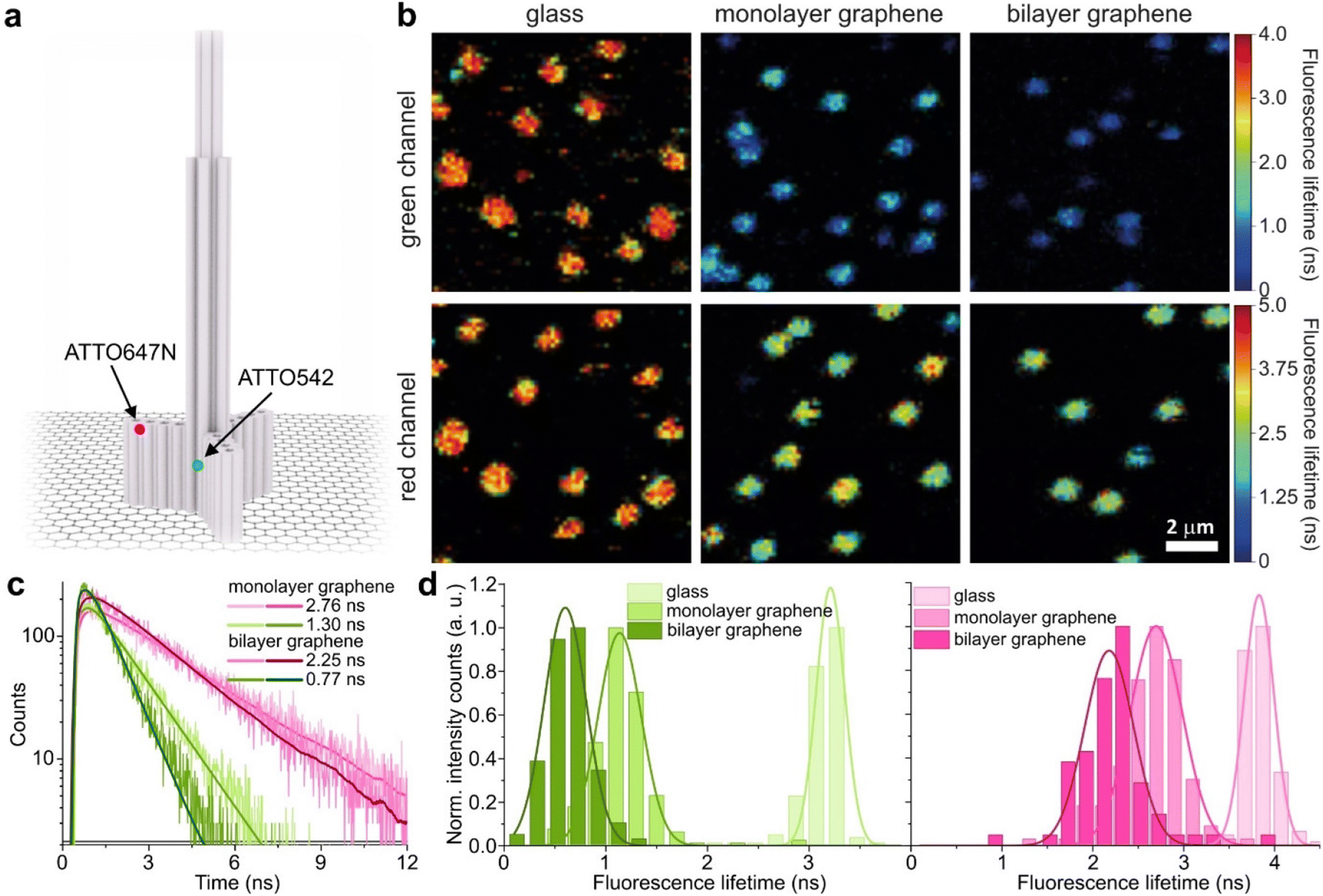 | ||
Fig. 1 (a) Sketch of a pillar-shaped DNA origami nanostructure immobilized on graphene, with the marked positions of dye molecules, dye ATTO542 (green) at the height of 16 nm and dye ATTO647N (magenta) at the height of 24 nm from the substrate surface. (b) Example fluorescence lifetime intensity maps (10 × 10 μm) obtained for DNA origami nanostructures (presented in sketch (a)) labeled with two dye molecules, a green dye ATTO542 (green channel, upper panels) and a red dye ATTO647N (red channel, lower panel) immobilized on glass (on the left), monolayer graphene (in the middle) and bilayer graphene (on the right). (c) Examples of fluorescence decays of colocalized green (green) and red (magenta) dye molecules positioned in DNA origami nanostructures immobilized on monolayer (bright shades) and bilayer graphene (dark shades) fitted with a monoexponential function. (d) Histograms of the fluorescence lifetime of colocalized dye molecules ATTO542 (green) and ATTO647N (magenta) positioned in DNA origami nanostructures immobilized on glass ( and and  ), and monolayer ( ), and monolayer ( and and  ) and bilayer graphene ( ) and bilayer graphene ( and and  ) fitted with a Gaussian function. ) fitted with a Gaussian function. | ||
While the results obtained for monolayer graphene are in agreement with previously published reports,7,13,19 it is clearly visible that the presence of the additional graphene layer leads to stronger fluorescence quenching.14 The data also indicate that the change of the energy transfer efficiency resulting from the presence of the second graphene layer is more pronounced for a dye at the height of 16 nm, which is closer to d0, the region of the highest distance sensitivity of GET (Fig. 1d). To quantify the effect of multiple layers, we carried out single-molecule fluorescence measurements for ten pillar-shaped DNA origami nanostructures immobilized on monolayer, bilayer and trilayer graphene, with two dye molecules, ATTO542 and ATTO647N, positioned at heights ranging from 12 to 53 nm. Fig. 2 displays the mean fluorescence lifetime values alongside their respective standard deviations, acquired from colocalized emitters across all measured samples. The corresponding spot-integrated fluorescence lifetime histogram and related results are shown in the ESI (Fig. S7†). The experimental data obtained for monolayer graphene (Fig. 2a) is fitted with the function 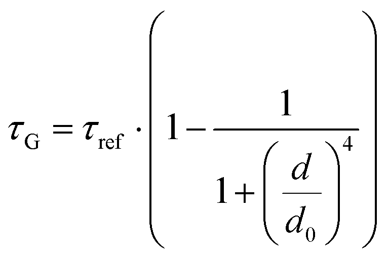 , where τref is the fluorescence lifetime of the reference sample measured on glass (mean value averaged from the reference measurements of all DNA origami nanostructures on glass), and is equal to 3.27 ± 0.19 ns for ATTO542 (green) and 3.81 ± 0.15 ns for ATTO647N (magenta), and d0 is the distance of 50% quenching efficiency (17.7 ± 0.5 nm for a green dye molecule and 18.5 ± 0.7 nm for a red dye molecule).13,19 Compared to our previously published work,13 we additionally carried out measurements for emitters positioned at heights of 30 and 40 nm from the graphene surface, to fill the gap for distances between 24 and 53 nm.
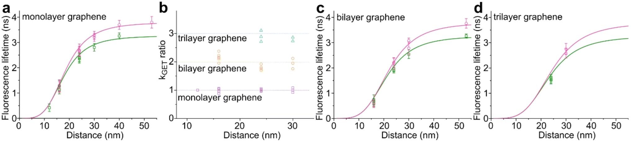 | ||
Fig. 2 Mean values with standard deviations of the fluorescence lifetime measured for colocalized dye molecules in DNA origami nanostructures. ATTO542 (green) and ATTO647N (magenta) were studied as a function of the distance from the surface: (a) monolayer, (c) bilayer, and (d) trilayer graphene. (b) The ratio of the energy transfer rates of multilayer graphene to monolayer graphene as a function of the distance, where the energy transfer rate is calculated via:  . Green (ATTO542) and magenta (ATTO647N) curves (a, c and d) are calculated using the equation . Green (ATTO542) and magenta (ATTO647N) curves (a, c and d) are calculated using the equation 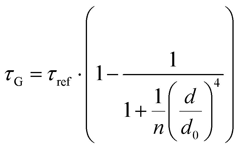 , as the function of the distance d between graphene and the emitter, where d0 is the distance of 50% quenching efficiency, and is equal to 17.7 ± 0.5 nm for green dyes and 18.5 ± 0.7 nm for red dyes,13 n is the number of graphene layers, and τref is the reference value of the fluorescence lifetime measured for DNA origami nanostructures immobilized on glass, and is equal to 3.27 ± 0.19 ns for ATTO542 and 3.81 ± 0.15 ns for ATTO647N. , as the function of the distance d between graphene and the emitter, where d0 is the distance of 50% quenching efficiency, and is equal to 17.7 ± 0.5 nm for green dyes and 18.5 ± 0.7 nm for red dyes,13 n is the number of graphene layers, and τref is the reference value of the fluorescence lifetime measured for DNA origami nanostructures immobilized on glass, and is equal to 3.27 ± 0.19 ns for ATTO542 and 3.81 ± 0.15 ns for ATTO647N. | ||
In order to better understand how the energy transfer process scales with the number of graphene layers, we calculated the energy transfer rate constants using the equation  (for more details, see the calculations in the ESI†). For each dye and each distance measured on monolayer graphene, we normalized the energy transfer rate constant by the corresponding energy transfer rate constant of monolayer graphene (Fig. 2b). The dashed lines indicate the ratio of the energy transfer rates equal to 1 (pink), 2 (orange) and 3 (blue). As all data points closely align at 1 for monolayer graphene, 2 for bilayer graphene, and 3 for trilayer graphene, regardless of the distance, we conclude that every additional graphene layer exhibits the same quenching behavior and the energy transfer rates are additive. Accordingly, multilayer graphene behaves as a stack of decoupled monolayer graphene sheets.14 Considering this, we extend the model for the graphene energy transfer, including this time the number of graphene layers (n), which results in the energy transfer efficiency:
 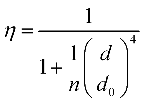 . Using this equation with the same parameters as above, and n = 2 or 3 for bilayer and trilayer graphene, respectively, we fitted the experimental fluorescence lifetimes (Fig. 2c and d). We obtained a very good quantitative agreement of the model with the experimental data in the entire distance range, confirming the appropriateness of the assumptions.
Dynamic assay for monolayer and bilayer GET
Graphene-on-glass coverslips emerge as a beautiful tool to visualize distance changes in the z-direction (axial dimension) in dynamic DNA origami nanostructures and bioassays, as well as for super-resolution imaging and tracking.7,9,12 In this contribution, we expand the dynamic range of GET by adding an additional graphene layer, creating bilayer graphene substrates. For studying the extended dynamic range in single-molecule biophysical experiments, we equipped the pillar-shaped DNA origami nanostructures with protruding ssDNA, a pointer of the length of 24 nucleotides (nt), labeled with Cy3B at its end (Fig. 3a). We placed the pointer at 28 or 35 nm above graphene (short names: P28 and P35). For each pointer, we designed two docking sites, ssDNA protruding from the DNA origami nanostructure 7 nm above and below the pointer, that have 7 nt complementary to the pointer sequence. Additionally, in all DNA origami nanostructures, we incorporated a red dye ATTO647N at the height of 16 nm as a reference probe to monitor both the quality of graphene and the number of layers. Pillar-shaped DNA origami nanostructures with P28 and P35 were measured on glass, and monolayer and bilayer graphene. For all samples, we measured fluorescence lifetime maps (examples in Fig. 3b and c, for the reference measurement see Fig. S10 in the ESI†). Using pulsed interleaved laser excitation at 532 and 639 nm, we quasi-simultaneously excited and measured both emitters incorporated in the DNA origami nanostructure, Cy3B and ATTO647N. As explained in the previous section of this article, the presence of both emitters indicates the proper folding of the DNA origami nanostructure, which is confirmed when spots on fluorescence lifetime maps representing single emitters are visible in both the green and red channels (upper and lower panels in Fig. 3b and c).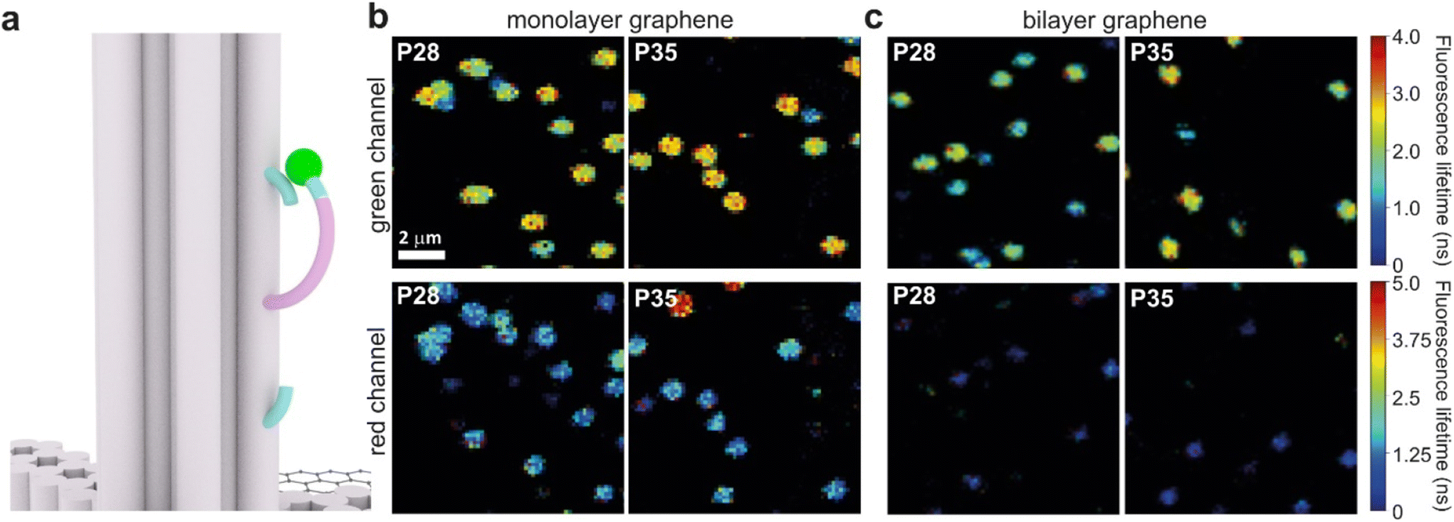 | ||
| Fig. 3 (a) Sketch of the dynamic assay incorporated in the pillar-shaped DNA origami nanostructure, with the marked positions of the ssDNA pointer P35 (purple + turquoise) at the height of 35 nm from the substrate surface labeled with a dye molecule Cy3B (green sphere), complementary via 7 nucleotides to two binding sites (turquoise) located 7 nm above and below the pointer. (b and c) Example fluorescence lifetime intensity maps (10 × 10 μm) were obtained for the pointers positioned at the height of 28 nm (P28) or 35 nm (P35), labeled with a dye Cy3B (green channel, upper panels) in the DNA origami nanostructures immobilized on (b) monolayer and (c) bilayer graphene. In all constructs, ATTO647N positioned at the height of 16 nm (not marked on the sketch) was used as an internal reference to monitor the quality of graphene (red channel, lower panels). | ||
Subsequently, for all selected spots, we recorded fluorescence intensity time traces (Fig. 4, for the reference measurements on glass check the ESI, Fig. S10 and S11†). In the case of P28, the transient binding of the pointer between both binding sites is resolved both on monolayer and bilayer graphene (Fig. 4a). In the second case, the contrast defined as the difference in the fluorescence lifetime between the two conformations increases from about 0.7 to 1.0 ns. Fluorescence decays of the upper and the lower binding sites obtained for the pointer P28 immobilized on bilayer graphene presented in Fig. 4a (fluorescence lifetime trace in pink) are depicted in Fig. S12.† Notably, for P35 measured on monolayer graphene, the fluorescence lifetime time traces (Fig. 4b) show similar intensity oscillations as those recorded on glass (Fig. S13†), thus it is not possible to distinguish the two conformations (histogram in Fig. S14b†). For the same construct immobilized and measured on bilayer graphene, the transient binding between lower and upper binding sites is resolved, and the fluorescence lifetime values switch between 2.1 and 2.6 ns (Fig. S14b†). The selection of these particular positions for placing ssDNA pointers was not arbitrary. Specifically, based on calculations (check more details in the ESI†), the positioning of the pointer at the height of 28 nm and its binding sites 7 nm above and below, yields the greatest difference in the fluorescence lifetime between mono- and bilayer graphene which corresponds to the maximum possible difference of the energy transfer efficiency value reaching 11% (Fig. S8 and S9†). Consequently, with such a system, we can achieve the highest resolution for bilayer graphene compared to monolayer graphene. Whereas the height of 35 nm was selected as it is the upper detection limit of GET for monolayer graphene, and the visualization of the dynamics processes at such a distance from monolayer graphene is not possible. However, by creating a bilayer graphene substrate, we can resolve these binding events. This proof-of-concept experiment demonstrates the capabilities of multilayer graphene for GET operating at a longer distance range which makes it feasible for larger constructs. Moreover, the region of the highest sensitivity for the dynamic system is shifted from about 16–17 to 19–21 nm (the position of the pointer, whose binding sites are located 7 nm below and above, see Fig. S8 and S9† in the ESI). By changing the number of graphene layers, it is possible to tailor the operating distance range of GET best suited to the studied systems.
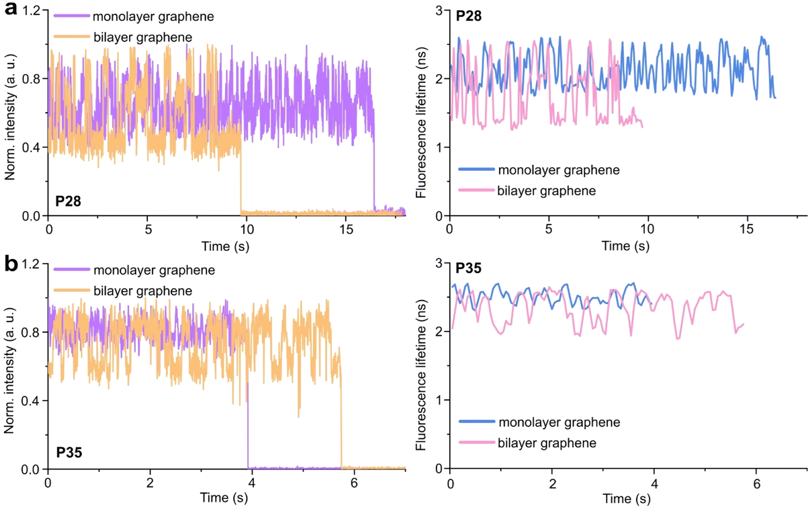 | ||
| Fig. 4 Examples of the measured fluorescence intensity (violet and orange) and the corresponding fluorescence lifetime (blue and pink) time traces obtained for the pointer assay (ssDNA) positioned at the heights of 28 nm – P28 (a) and 35 nm – P35 (b), labeled with a dye molecule Cy3B, incorporated in the pillar-shaped DNA origami nanostructure immobilized on monolayer (violet → blue) and bilayer (orange → pink) graphene. | ||
Conclusions
The study investigated the influence of the number of graphene layers on graphene energy transfer (GET) efficiency, particularly focusing on monolayer, bilayer, and trilayer graphene substrates. Each additional graphene layer led to stronger fluorescence quenching, indicating enhanced GET efficiency and suggesting a potential extension of the dynamic working range of GET. Precise measurements using DNA origami nanostructures labeled with dye molecules positioned at various distances from the graphene surface reaffirmed a distance scaling law for GET, validating the d−4 scaling law and the characteristic distance for 50% energy transfer efficiency (d0). Moreover, the study highlighted the additive effect of graphene layers on the overall energy transfer rate, indicating the potential for tailored control over GET efficiency based on the number of graphene layers. Additionally, a dynamic assay utilizing bilayer graphene substrates was introduced to enhance the resolution of GET (extend the sensitive distance range), aiming to resolve binding events with higher precision compared to monolayer graphene. Results demonstrated the feasibility of resolving such events at distances beyond the capability of monolayer graphene, showcasing the potential of bilayer graphene substrates for achieving enhanced resolution in dynamic assays employing GET. Overall, these findings contribute to advancing our understanding of graphene's optoelectronic properties, particularly in the context of energy transfer processes, and offer valuable insights for the development of graphene-based technologies in various fields. For biosensing, where yes/no answers instead of exact quantification are required, bilayer graphene closes the holes frequently found in monolayer graphene and can make graphene chips more reliable for optical biosensing. Further exploration of graphene-layer-dependent effects on energy transfer mechanisms holds promise for optimizing graphene-based devices and expanding their applicability in biosensing and super-resolution microscopy.Author contributions
The manuscript was written through contributions of all authors. All authors have given approval to the final version of the manuscript.Conflicts of interest
The authors declare no competing financial interest.Acknowledgements
Many thanks to Renukka Yaadav for preparing sketches of DNA origami nanostrucutres, to Dr. Tim Schröder for fruitful discussions, and to Dr. Alan Szalai and Giovanni Ferrari for writing the Python software smPyFLIM used for the analysis of the data obtained with the TCSPC module. IK and KG acknowledge support by the National Science Center (Sonata 2019/35/D/ST5/00958). The authors are thankful for financial support from the Deutsche Forschungsgemeinschaft (DFG, German Research Foundation) under Grant Numbers TI 329/14-1 and KA 5449/2-1, and from the Center for NanoScience (CeNS).References
- K. S. Novoselov, A. Geim, S. V. Morozov, D. Jiang, Y. Zhang, S. V. Dubonos, I. V. Grigorieva and A. A. Firsov, Science, 2004, 306, 666–669 CrossRef CAS PubMed.
- A. C. Ferrari, F. Bonaccorso, V. Fal'ko, K. S. Novoselov, S. Roche, P. Bøggild, S. Borini, F. H. L. Koppens, V. Palermo, N. Pugno, J. A. Garrido, R. Sordan, A. Bianco, L. Ballerini, M. Prato, E. Lidorikis, J. Kivioja, C. Marinelli, T. Ryhänen, A. Morpurgo, J. N. Coleman, V. Nicolosi, L. Colombo, A. Fert, M. Garcia-Hernandez, A. Bachtold, G. F. Schneider, F. Guinea, C. Dekker, M. Barbone, Z. Sun, C. Galiotis, A. N. Grigorenko, G. Konstantatos, A. Kis, M. Katsnelson, L. Vandersypen, A. Loiseau, V. Morandi, D. Neumaier, E. Treossi, V. Pellegrini, M. Polini, A. Tredicucci, G. M. Williams, B. Hee Hong, J. H. Ahn, J. Min Kim, H. Zirath, B. J. Van Wees, H. Van Der Zant, L. Occhipinti, A. Di Matteo, I. A. Kinloch, T. Seyller, E. Quesnel, X. Feng, K. Teo, N. Rupesinghe, P. Hakonen, S. R. T. Neil, Q. Tannock, T. Löfwander and J. Kinaret, Nanoscale, 2015, 7, 4598–4810 RSC.
- R. Ye and J. M. Tour, ACS Nano, 2019, 13, 10872–10878 CrossRef CAS PubMed.
- R. R. Nair, P. Blake, A. N. Grigorenko, K. S. Novoselov, T. J. Booth, T. Stauber, N. M. R. Peres and A. K. Geim, Science, 2008, 320, 1308 CrossRef CAS PubMed.
- J. Wang, F. Ma, W. Liang, R. Wang and M. Sun, Nanophotonics, 2017, 6, 943–976 CrossRef CAS.
- R. Kumar, D. P. Singh, R. Muñoz, M. Amami, R. K. Singh, S. Singh and V. Kumar, Mater. Today Chem., 2023, 33, 101750 CrossRef CAS.
- I. Kamińska, J. Bohlen, R. Yaadav, P. Schüler, M. Raab, T. Schröder, J. Zähringer, K. Zielonka, S. Krause and P. Tinnefeld, Adv. Mater., 2021, 33, 2101099 CrossRef PubMed.
- A. Ghosh, A. Sharma, A. I. Chizhik, S. Isbaner, D. Ruhlandt, R. Tsukanov, I. Gregor, N. Karedla and J. Enderlein, Nat. Photonics, 2019, 13, 860–865 CrossRef CAS.
- A. M. Szalai, G. Ferrari, L. Richter, J. Hartmann, M.-Z. Kesici, B. Ji, K. Coshic, A. Jaeger, A. Aksimentiev, I. Tessmer, I. Kamińska, A. M. Vera and P. Tinnefeld, biorxiv.
- N. Füllbrunn, Z. Li, L. Jorde, C. P. Richter, R. Kurre, L. Langemeyer, C. Yu, C. Meyer, J. Enderlein, C. Ungermann, J. Piehler and C. You, Elife.
- R. M. R. Adão, R. Campos, E. Figueiras, P. Alpuim and J. B. Nieder, 2D Mater., 2019, 6, 045056 CrossRef.
- J. Zähringer, F. Cole, J. Bohlen, F. Steiner, I. Kamińska and P. Tinnefeld, Light: Sci. Appl., 2023, 12, 1–8 CrossRef PubMed.
- I. Kaminska, J. Bohlen, S. Rocchetti, F. Selbach, G. P. Acuna and P. Tinnefeld, Nano Lett., 2019, 19, 4257–4262 CrossRef CAS PubMed.
- Z. Chen, S. Berciaud, C. Nuckolls, T. F. Heinz and L. E. Brus, ACS Nano, 2010, 4, 2964–2968 CrossRef CAS PubMed.
- A. Raja, A. Montoya-Castillo, J. Zultak, X. X. Zhang, Z. Ye, C. Roquelet, D. A. Chenet, A. M. Van Der Zande, P. Huang, S. Jockusch, J. Hone, D. R. Reichman, L. E. Brus and T. F. Heinz, Nano Lett., 2016, 16, 2328–2333 CrossRef CAS PubMed.
- R. S. Swathi and K. L. Sebastian, J. Chem. Phys., 2009, 130, 086101 CrossRef CAS PubMed.
- R. S. Swathi and K. L. Sebastian, J. Chem. Phys., 2008, 129, 054703 CrossRef CAS PubMed.
- F. Federspiel, G. Froehlicher, M. Nasilowski, S. Pedetti, A. Mahmood, B. Doudin, P. Serin, J. Lee, D. Halley, B. Dubertret, P. Gilliot and S. Berciaud, Nano Lett., 2015, 15, 1252–1258 CrossRef CAS PubMed.
- L. Gaudreau, K. J. Tielrooij, G. E. D. K. Prawiroatmodjo, J. Osmond, F. J. García de Abajo and F. H. L. Koppens, Nano Lett., 2013, 13, 2030–2035 CrossRef CAS PubMed.
- T. Ohta, A. Bostwick, T. Seyller, K. Horn and E. Rotenberg, Science, 2006, 313, 951–954 CrossRef CAS PubMed.
- Y. Sui and J. Appenzeller, Nano Lett., 2009, 9, 2973–2977 CrossRef CAS PubMed.
- A. Yacoby, Nat. Phys., 2011, 7, 925–926 Search PubMed.
- S. Krause, E. Ploetz, J. Bohlen, P. Schuler, R. Yaadav, F. Selbach, F. Steiner, I. Kamińska and P. Tinnefeld, ACS Nano, 2021, 15, 6430–6438 CrossRef CAS PubMed.
Footnotes |
| † Electronic supplementary information (ESI) available: Detailed information on DNA origami design, DNA origami folding and immobilization, measurement setups, fluorescence, Raman and SEM imaging, Raman spectra measurements, calculations, and analysis. See DOI: https://doi.org/10.1039/d4nr01723d |
| ‡ Current address: Paul Scherrer Institut, 5232 Villigen PSI, Switzerland. |
| This journal is © The Royal Society of Chemistry 2024 |