
A perylene diimide based polymer: a dual function interfacial material for efficient perovskite solar cells†
Fanqi
Meng
a,
Kuan
Liu
ab,
Shuixing
Dai
a,
Jiangjian
Shi
b,
Huiyin
Zhang
b,
Xin
Xu
b,
Dongmei
Li
*b and
Xiaowei
Zhan
 *a
*a
aDepartment of Materials Science and Engineering, College of Engineering, Key Laboratory of Polymer Chemistry and Physics of Ministry of Education, Peking University, Beijing 100871, China. E-mail: xwzhan@pku.edu.cn
bCAS Key Laboratory for Renewable Energy, Beijing Key Laboratory for New Energy Materials and Devices, Institute of Physics, Chinese Academy of Sciences, Beijing 100190, China. E-mail: dmli@iphy.ac.cn
First published on 14th December 2016
Abstract
An n-type semiconducting copolymer of perylene diimide and dithienothiophene (PPDIDTT) is used as a dual function interfacial layer to modify the surface of perovskite films in inverted perovskite solar cells. The PPDIDTT layer can remarkably passivate the surface trap states of perovskite through the formation of a Lewis adduct between the under-coordinated Pb in perovskite and S in the dithienothiophene unit of PPDIDTT, and also shows efficient charge extraction and transfer properties. The PPDIDTT modified devices exhibit a maximum power conversion efficiency of 16.5%, superior to that of the control devices without PPDIDTT (15.3%). In addition, the device stability and hysteresis in J–V curves of the modified devices are also improved compared to those of the control devices.
Introduction
In the past few years, solar cells using organic–inorganic hybrid perovskites (e.g., methylammonium lead halides CH3NH3PbX3, where X = Cl−, I−, Br−) as photoactive layers have received increasing attention, because of their broad absorption spectrum from the visible to the near-infrared region, ambipolar charge transport, long carrier diffusion length and lifetime.1–5 In addition, organometallic halide perovskite materials allow for solution processing at room temperature, which makes it possible to achieve low-cost and large-scale fabrication, hence competitiveness in a future commercialization scenario. Since their first incorporation as sensitizers in dye-sensitized solar cells by Miyasaka et al. in 2009,6 the power conversion efficiency (PCE) of organic–inorganic hybrid perovskite based solar cells has increased from 3.8% to over 20% with an unbelievable speed, thanks to the development of different processing techniques, device architectures and novel materials.7–16Perovskite solar cells (PSCs) consist of an organometallic halide perovskite light-absorbing layer sandwiched between hole and electron transporting layers (ETLs), which are in contact with two electrodes. To date, most state-of-the-art PSCs employ a conventional structure with mesoporous TiO2 as an electron transporting material and involve a high-temperature (up to 500 °C) sintering process of mesoporous TiO2, which leads to a complicated fabrication process, high cost and incompatibility with flexible/plastic substrates. Therefore, low-temperature processing and a simple device architecture are desirable for its further commercial applications.17–21 In 2013, Guo et al. reported inverted planar heterojunction PSCs using poly(3,4-ethylenedioxythiophene):poly(styrene sulfonate) (PEDOT:PSS) and [6,6]-phenyl-C61-butyric acid methyl ester (PC61BM) as hole and electron transporting materials, respectively.22 PCEs as high as 19.4% and a certified PCE of 18.21% (1 cm2) were achieved for the inverted PSCs, comparable to those of conventional PSCs.23–31
The trap states are one of the key factors limiting the further increase of the device performance.32–34 Trap states in perovskites generally stem from surface and bulk defects, which could induce carrier loss and deteriorate the performance of the PSCs.35–38 The vacancies of halides could be the origin of surface and bulk defects. The loss of halide ions leads to under-coordinated Pb atoms or clusters in some cases, which may become carrier recombination centers and decrease the current density and fill factor (FF), and also may be a reason for the occurrence of hysteresis phenomenon.35,39,40 Therefore, it is necessary to develop effective methods to passivate the trap states to further promote the performance of PSCs. A convenient way to passivate surface defects of under-coordinated Pb is to treat the perovskite film with nitrogen-containing materials, which can provide lone pair electrons to form coordination bonds with under-coordinated Pb atoms. For example, pyridine,33,35 amino-functionalized fullerenes,37 amino-functionalized graphene,41 and amino-silane42 were used to modify the surface of perovskites in PSCs, which exhibited PCEs of up to 14.6%. However, the device performance after these treatments is still not high. Therefore, the development of more efficient trap-passivating materials for high-efficiency PSCs is necessary.
In this work, we demonstrate the first example for the application of perylene diimide polymers in PSCs. Perylene diimide polymers are classical n-type organic semiconductors and exhibit high performance in organic electronic devices, such as field-effect transistors and organic solar cells,43,44 but have not been used in PSCs. We used a copolymer of perylene diimide and dithienothiophene (DTT), PPDIDTT (Fig. S1, ESI†), as a dual function interfacial material to modify the surface of perovskite films in inverted PSCs. PPDIDTT exhibits high electron mobility, strong absorption from the visible to the near-infrared region and a similar LUMO energy level to that of PC61BM.45 The matched LUMO energy level and high electron mobility are beneficial for the extraction of photogenerated electrons from perovskite films and transfer to ETLs. Moreover, the electron-rich DTT unit in PPDIDTT, as the Lewis base, can well passivate the under-coordinated Pb in CH3NH3PbI3−xClx (MAPbI3−xClx) via the coordination between the Lewis acid and the Lewis base (Fig. 1).33,35,46 Unlike the common passivants in inverted PSCs, such as PC61BM, which act as a Lewis acid to passivate the halide-induced traps under a long annealing process,47 the trap-passivation process of PPDIDTT is carried out at room temperature. After treatment with PPDIDTT, the inverted PSCs exhibit a maximum PCE of 16.5%, superior to that of the control devices without a PPDIDTT interfacial layer (15.3%). In addition, compared with the control devices, the device stability of the modified devices is also enhanced.
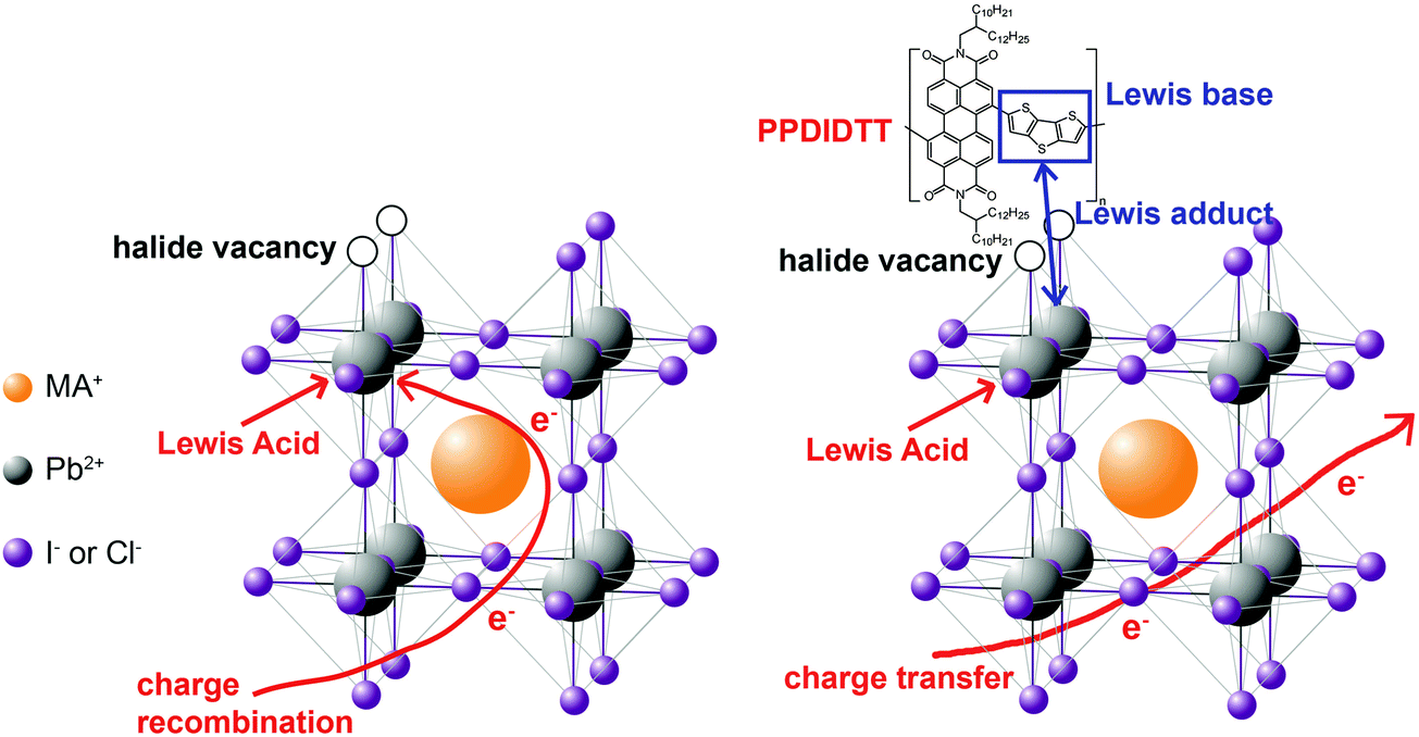 | ||
| Fig. 1 Schematic illustration of the interaction between under-coordinated Pb and the DTT unit in PPDIDTT. | ||
Results and discussion
Surface morphology
An ultrathin PPDIDTT interfacial layer was deposited on the top of the perovskite film by spin-coating its chloroform solution at an appropriate concentration. A 50 nm thick PC61BM ETL was subsequently deposited on the top of the interfacial layer. The surface morphologies of different films are characterized by atomic force microscopy (AFM). The neat perovskite film exhibits a typical polycrystalline structure with multiple grains (Fig. 2a). The root-mean-square (RMS) roughness of the neat perovskite film is calculated to be 43.5 nm. The PPDIDTT coated perovskite film also shows a typical morphology with a slightly decreased RMS roughness of 41.9 nm, indicating the existence of an ultrathin PPDIDTT interfacial layer (Fig. 2b). Fig. 2c and d represent the topographical images of perovskite/PC61BM and perovskite/PPDIDTT/PC61BM films, respectively. Both of them show amorphous and smoother morphologies of PC61BM with reduced RMS roughness values of 17.3 and 11.7 nm, respectively. The introduction of a PPDIDTT interfacial layer leads to a smoother PC61BM ETL with a better coverage. Although PPDIDTT shows strong absorption from the visible to the near-infrared region, the absorption spectrum of the PPDIDTT modified perovskite film is almost identical to that of the neat perovskite film (Fig. S2, ESI†), also suggesting that the interfacial layer is indeed ultrathin.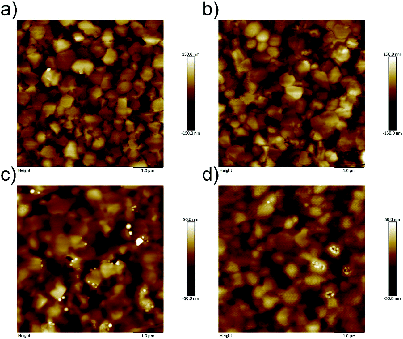 | ||
| Fig. 2 AFM images of (a) neat perovskite film, (b) PPDIDTT coated perovskite film, (c) perovskite/PC61BM film, and (d) perovskite/PPDIDTT/PC61BM film. | ||
Trap passivation and electron extraction
In order to investigate the interaction between PPDIDTT and the perovskite film, Fourier transform infrared (FTIR) spectroscopy is employed to analyze the MAPbI3−xClx powder, the PPDIDTT powder and the blended PPDIDTT:MAPbI3−xClx powder. To distinguish the difference in the spectra between PPDIDTT and PPDIDTT:MAPbI3−xClx, the spectra are normalized according to the peak of 1246 cm−1, which is assigned to the in-plane perylene diimide ring deformation and is thus insensitive to Pb.48 As shown in Fig. 3a, for the neat PPDIDTT powder, the peaks at 861 and 839 cm−1 are assigned to the antisymmetric C–S stretching and symmetric C–S stretching modes, respectively.49,50 The FTIR spectrum of the blended PPDIDTT:MAPbI3−xClx powder shows weaker ν(C–S) (861 and 839 cm−1) (inset diagram in Fig. 3a), which confirms the presence of interaction between the DTT unit and MAPbI3−xClx.49,51 Raman spectroscopy is further employed to analyze the interaction between MAPbI3−xClx and PPDIDTT. Two new weak Raman bands at 215 cm−1 and 234 cm−1 are assigned to Pb–S stretching, which is direct evidence of the formation of a Lewis adduct between the under-coordinated Pb in the MAPbI3−xClx film and S in the DTT unit of PPDIDTT.52 It should be noted that the samples for FTIR and Raman spectra measurements were prepared at room temperature, indicating that this interaction between MAPbI3−xClx and PPDIDTT is still efficient without any thermal treatment, unlike the widely reported fullerene based passivants.47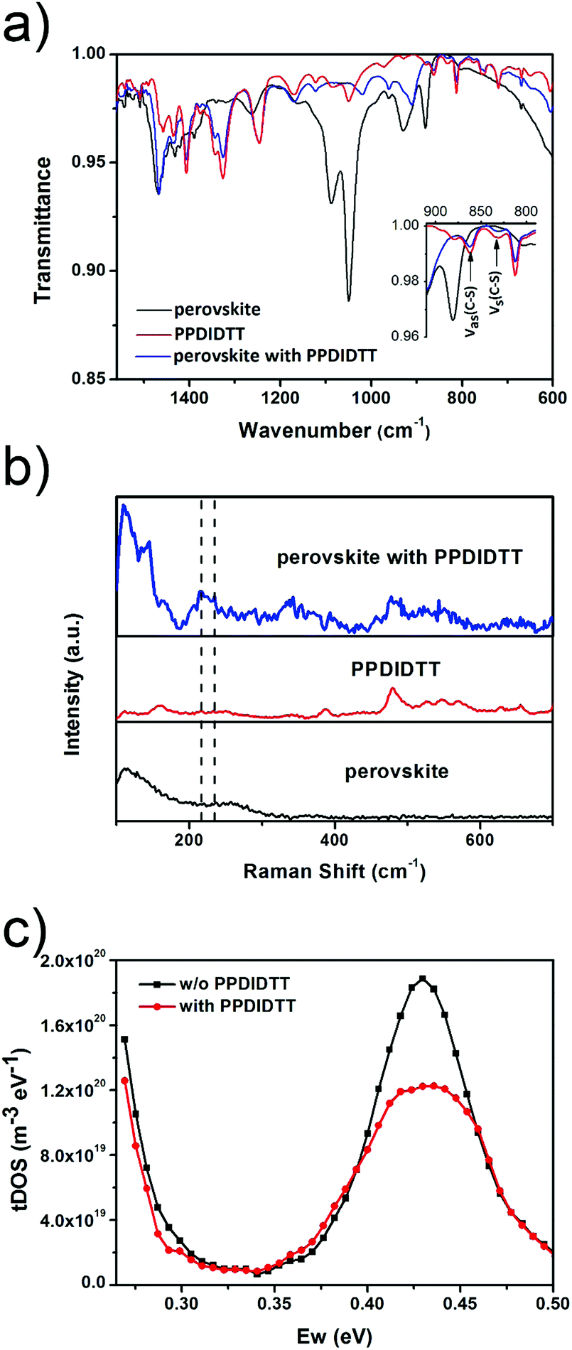 | ||
| Fig. 3 (a) FTIR spectra of the neat MAPbI3−xClx, neat PPDIDTT and blended PPDIDTT:MAPbI3−xClx. Inset: enlarged FTIR spectra in the wavenumber from 910 to 790 cm−1. (b) Raman spectra of the PPDIDTT coated MAPbI3−xClx film, neat PPDIDTT film and the neat perovskite film. (c) tDOS of inverted MAPbI3−xClx based PSCs with and without the PPDIDTT interfacial layer. | ||
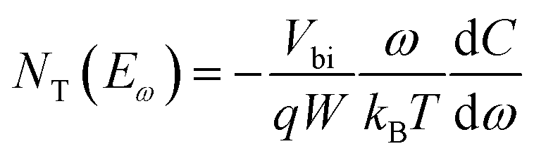
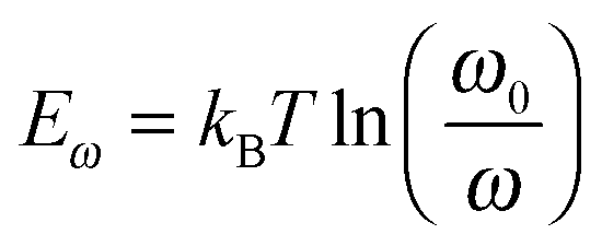
Thermal admittance spectroscopy (TAS) analysis is employed to quantize the reduction of trap states in perovskite films caused by the passivation of PPDIDTT. TAS is a well-established, effective technique for characterizing both shallow and deep defects, which has been widely applied for understanding defects in organic solar cells and PSCs.53,54 The energetic profile of trap density of states (tDOSs) can be derived from the angular frequency dependent capacitance using the equation:
where ω0 is the attempt-to-escape frequency. The trap states below the energy demarcation can capture or emit charges with the given ω and contribute to the capacitance. As shown in Fig. 3c, the neat perovskite film exhibits a relatively large tDOS (2 × 10¹⁹ to 2 × 10²⁰ m−3 eV−1). The tDOS of the PPDIDTT modified devices decreases by around 50% in the energy depth of 0.40–0.45 eV, while the tDOS in the energy depth below 0.40 eV decreases slightly, which indicates that the passivation of the PPDIDTT interfacial layer mainly occurs at the surface of perovskites (efficient passivation of deep traps), as shown in Fig. 1b.54
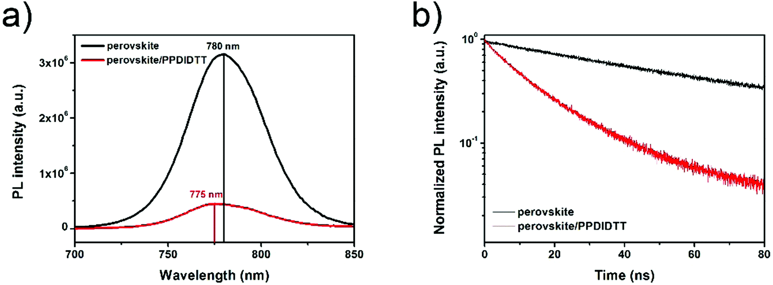
In order to investigate the charge transfer process between the perovskite film and the PPDIDTT interfacial layer, steady-state and time-resolved photoluminescence (PL) were employed. The PL light excitation region is confined close to the surface of the perovskite film by choosing a short wavelength of 550 nm. As shown in Fig. 4a, the neat perovskite film shows the PL peak at 780 nm. After modifying the surface of the perovskite with PPDIDTT, a significant PL quenching of 86% is observed, indicating efficient electron extraction from perovskite to PPDIDTT. On the other hand, a blue-shift of the PL peak from 780 to 775 nm is observed for the perovskite/PPDIDTT film. The presence of trap states can cause band bending close to the surface of the perovskite film, leading to an apparent band gap lower than that of the bulk with a red-shifted PL peak. Filling the trap states enables the recovery of the bandgap and blue-shifts the PL peak.54 The PL results also confirm the trap-passivation properties of the PPDIDTT interfacial layer by filling the deep traps at room temperature. In contrast, the PL peak of the perovskite/PC61BM film is still located at 780 nm without any blue-shift (Fig. S3a, ESI†), indicating the inferior trap-passivation ability of PC61BM at room temperature.
 | ||
| Fig. 4 (a) Steady-state and (b) time-resolved transient PL spectra of neat perovskite and perovskite/PPDIDTT films. | ||
The time-resolved PL transient spectra were used to study electron extraction from perovskite to PPDIDTT. As shown in Fig. 4b, the neat perovskite film exhibits an average decay time of 61.3 ns fitted with a bi-exponential decay function. After modifying the surface of perovskite with PPDIDTT, the sample exhibits a much faster PL quenching, with an average decay time of 14.7 ns. The perovskite/PDIDTT/PC61BM film also exhibits faster PL quenching with an average decay time of 2.8 ns, compared with that of the perovskite/PC61BM film (3.9 ns), indicating a better electron-extraction ability of the PPDIDTT/PC61BM bilayer compared with the neat PC61BM ETL (Fig. S3b, ESI†). Therefore, TAS, steady-state and time-resolved PL results demonstrate that the PPDIDTT interfacial layer can act as a dual-function modification layer for PSCs, which not only efficiently passivates deep traps of the perovskite but also efficiently extracts photogenerated electrons from the perovskite and transfers to the PC61BM ETL.
Device performance
We fabricated inverted planar heterojunction PSCs with a configuration of ITO/PEDOT:PSS/MAPbI3−xClx/PPDIDTT/PC61BM/Bphen/Ag (Fig. 5a). Fig. 5b shows the cross-sectional scanning electron microscopy (SEM) image of the representative device. The total thickness of the device is around 560 nm, consisting of a 30 nm PEDOT:PSS hole transporting layer, a 400 nm perovskite film, a 50 nm PC61BM ETL and an 80 nm Ag counter electrode. The thicknesses of the PPDIDTT interfacial layer and the bathophenanthroline (Bphen) buffer layer are negligible. Fig. 5c shows the energy level diagram of the corresponding components in the devices. The LUMO energy level of PPDIDTT matches well with the conduction band of the MAPbI3−xClx perovskite and the LUMO energy level of PC61BM, which is beneficial for the extraction of photogenerated electrons from the perovskite film. An ultrathin Bphen buffer layer was deposited between the PC61BM ETL and the Ag counter electrode. The HOMO energy level of Bphen is deeper than the valence band of the MAPbI3−xClx perovskite, which is beneficial to the inhibition of photogenerated holes from the perovskite film to the Ag counter electrode and thus suppresses charge recombination.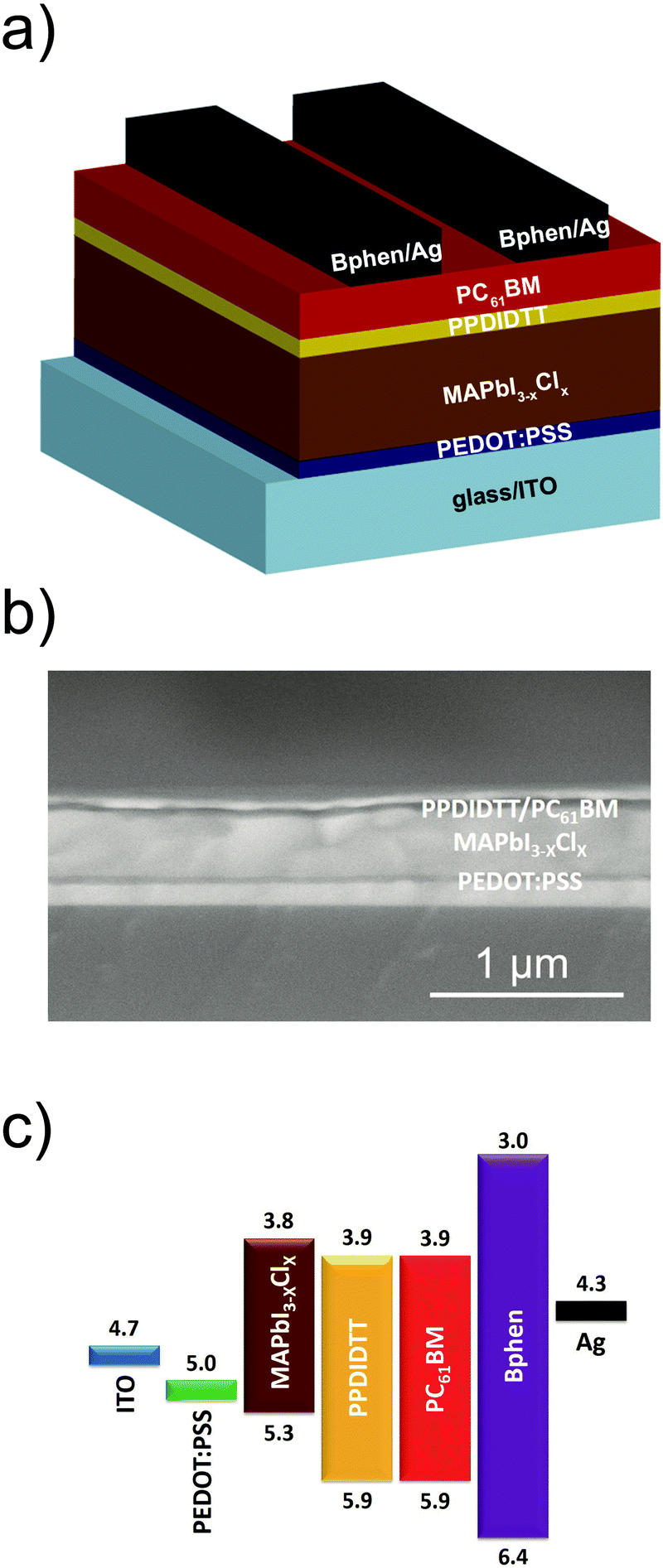 | ||
| Fig. 5 (a) Schematic device structure of inverted PSCs with the PPDIDTT interfacial layer. (b) Cross-sectional SEM image of the representative device. (c) Energy levels diagram of the corresponding components in the devices. | ||
The influence of the thickness of the PPDIDTT interfacial layer on the performance of inverted PSCs is investigated. Since the thickness of the PPDIDTT interfacial layer is hard to measure from SEM, the thickness of the PPDIDTT layer is basically controlled by varying the concentration of the PPDIDTT solution. Fig. S3 (ESI†) shows the J–V curves of the modified devices with the PPDIDTT interfacial layer deposited with its solution under different concentrations (from 5 mg mL−1 to 0.2 mg mL−1), and the detailed device performance parameters are summarized in Table S1 (ESI†). An optimal PPDIDTT thickness is based on the concentration of 0.5 mg mL−1; increasing the thickness leads to a lower short-circuit current density (JSC) and a lower FF mainly due to higher series resistance, while decreasing the thickness leads to weaker trap-passivation, electron-extraction and lower JSC.
With the introduction of the dual-function PPDIDTT interfacial layer, the modified devices exhibit a maximum PCE of 16.5%, with a JSC of 21.1 mA cm−2, a VOC of 990 mV and a vFF of 79.1% (Fig. 6a). For comparison, the control devices exhibit a maximum PCE of 15.3%, with a JSC of 20.3 mA cm−2, a VOC of 980 mV and a FF of 76.8% (Table 1). The enhanced PCE of the PPDIDTT modified devices can be attributed to efficient trap passivation and electron extraction of the PPDIDTT interfacial layer. The external quantum efficiency (EQE) of the inverted PSCs with the PPDIDTT interfacial layer is higher than that of the control devices without PPDIDTT, which is consistent with the profile of the JSC (Fig. 6b). In order to evaluate the accuracy of the measured photovoltaic performance, the calculated JSC values are obtained by integration of the EQE spectra. Both of them show a mismatch lower than 5% compared with J–V measurements.
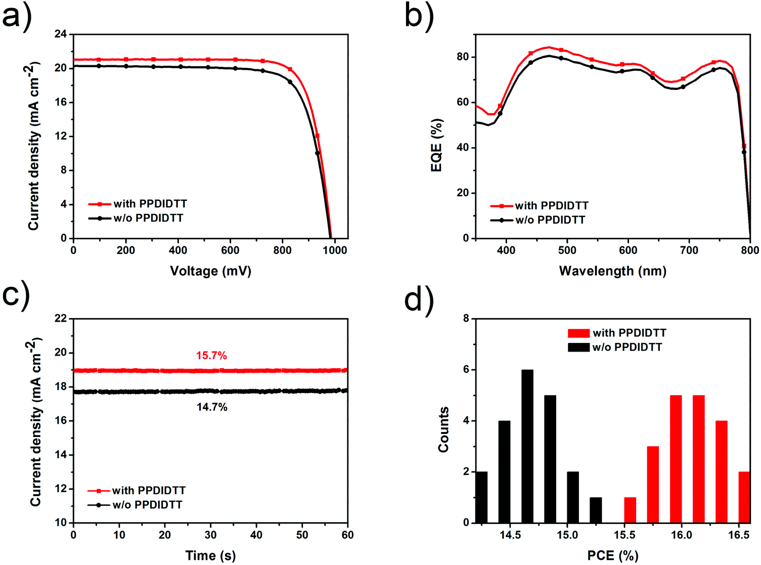 | ||
| Fig. 6 (a) The J–V curves, (b) EQE spectra and (c) steady-state current density and power output of the best-performing inverted PSCs with and without the PPDIDTT interfacial layer. (d) Statistical PCE distribution histogram of 20 individual modified devices with the PPDIDTT interfacial layer and control devices without PPDIDTT in the same batch. | ||
| Conditions | J SC (mA cm−2) | Calculated JSC (mA cm−2) | V OC (mV) | FF (%) | PCE (%) | |
|---|---|---|---|---|---|---|
| Average | Best | |||||
| Modified devices | 21.1 | 20.3 | 990 | 79.1 | 16.1 | 16.5 |
| Control devices | 20.3 | 19.4 | 980 | 76.9 | 14.7 | 15.3 |
Fig. 6c shows the steady-state JSC output of the inverted PSCs with and without the PPDIDTT interfacial layer under the maximum power point. The modified device exhibits a stabilized efficiency of 15.7%, superior to that of the control device without PPDIDTT (14.7%). Both of the stabilized efficiencies match well with those from J–V measurements. 20 devices modified with PPDIDTT exhibit an average PCE of around 16%; the reliability and repeatability of the device performance are improved due to the trap-passivation and electron-extraction of the PPDIDTT interfacial layer (Fig. 6d).
Fig. S5 (ESI†) shows the hysteresis effect in the J–V curves of inverted PSCs with and without the PPDIDTT interfacial layer. Obviously, PPDIDTT modified devices show almost the same J–V curves under forward and backward scanning, whereas obvious hysteresis in J–V curves is observed for the control device without PPDIDTT. The trap states in the perovskite/ETL interface are one of the origins of the photocurrent hysteresis in PCBM-based PSCs.44,53 Therefore, the reduction of the trap states facilitates elimination or reduction of the hysteresis effect. Fig. S6 (ESI†) shows the normalized PCE degradation curves of 10 individual devices with and without PPDIDTT in an inert atmosphere. The average normalized PCE of unencapsulated PPDIDTT modified devices can maintain over 110% of the initial value after 480 h storage. However, the average normalized PCE of the unencapsulated control devices without PPDIDTT maintains around 100% of the initial value under the same conditions. The enhanced stability of the modified devices may be related to the surface passivation of the perovskite film by the PPDIDTT interfacial layer.
Conclusions
We introduced an n-type perylene diimide based polymer, PPDIDTT, into the inverted PSCs as a dual function interfacial layer between the perovskite and the PC61BM ETL. The electron-donating DTT unit in PPDIDTT acts as a Lewis base to passivate the trap states on the surface of MAPbI3−xClx through the formation of a Lewis adduct of Pb and S, which is confirmed by FTIR and Raman spectral measurements. TAS and PL measurements indicate that the PPDIDTT interfacial layer efficiently passivates deep traps at the surface of the perovskite. Steady-state and time-resolved PL spectra reveal that the n-type semiconducting PPDIDTT is beneficial for efficient electron extraction from the perovskite film and transfer to the ETL due to the matched LUMO energy level and high electron mobility. Benefited from the trap-passivation and electron-extraction of the PPDIDTT interfacial layer, the inverted PSCs with the PPDIDTT interfacial layer exhibit a maximum PCE of 16.5%, superior to that of the control devices without PPDIDTT (15.3%); the stability, reliability and repeatability of the device performance as well as hysteresis in J–V curves are also improved. This work demonstrates that perylene diimide based polymers are promising interfacial materials for stable, high-performance PSCs with a negligible hysteresis effect.Experimental section
Materials
Unless stated otherwise, solvents and chemicals were obtained commercially and were used without further purification. PPDIDTT was synthesized according to our previous literature.45 PC61BM was purchased from American dye Inc. Bphen and PbI2 were purchased from Sigma-Aldrich Inc. N,N-dimethylformide (DMF), dimethylsulfoxide (DMSO) and chlorobenzene (CB) were purchased from Alfar Aesar. Isopropanol (IPA) was purchased from J&K Scientific Ltd. Methylamine (AR, 27% in methanol) was purchased from Sinopharm Chemical Reagent Co. Ltd. Methylammonium iodide (MAI) and methylammonium chloride (MACl) were synthesized according to the previous literature.55–57Device fabrication
Perovskite solar cells were fabricated by the following procedure. First of all, an indium tin oxide (ITO) glass substrate (sheet resistance = 15 Ω □−1) was cleaned in an ultrasonic bath of soap water, deionized water, acetone and ethanol for 20 min each, and treated in an ultraviolet-ozone chamber for 20 min. Next, a thin layer (30 nm) of PEDOT:PSS (Baytron PVP AI 4083, Germany) was spin-coated onto the ITO glass at a speed of 4000 rpm for 30 s and annealed at 130 °C for 20 min. Then, the MAPbI3−xClx based perovskite layer was deposited using a sequential deposition method according to the previous literature.58 1.25 M PbI2 was dissolved in a mixture solvent of DMF and DMSO (v/v = 9![[thin space (1/6-em)]](https://www.rsc.org/images/entities/char_2009.gif) :1) and stirred at room temperature. MAI and MACl (m/m = 9:1) were dissolved in IPA with a total concentration of 30 mg mL−1. The PbI2 solution was spin-coated on the ITO/PEDOT:PSS substrate at a speed of 3000 rpm for 60 s and heated at 70 °C to remove the solvent. After cooling down to room temperature, the mixture solution of MAI and MACl was spin-coated onto the PbI2 film at a speed of 4000 rpm for 20 s. The perovskite film was annealed at 85 °C for 1 h. PPDIDTT was dissolved in chloroform (CF) with different concentrations (5, 2, 1, 0.5 and 0.2 mg mL−1) and spin-coated on the top of the perovskite film at a speed of 3000 rpm for 30 s. Subsequently, PC61BM (dissolved in CB, 20 mg mL−1) and Bphen (dissolved in IPA, 0.5 mg mL−1) were spin-coated at a speed of 1000 rpm for 60 s and 3000 rpm for 30 s, respectively. Finally, an 80 nm thick Ag counter electrode was deposited on the top of the buffer layer by thermal evaporation at the pressure of 10−6 Torr.
:1) and stirred at room temperature. MAI and MACl (m/m = 9:1) were dissolved in IPA with a total concentration of 30 mg mL−1. The PbI2 solution was spin-coated on the ITO/PEDOT:PSS substrate at a speed of 3000 rpm for 60 s and heated at 70 °C to remove the solvent. After cooling down to room temperature, the mixture solution of MAI and MACl was spin-coated onto the PbI2 film at a speed of 4000 rpm for 20 s. The perovskite film was annealed at 85 °C for 1 h. PPDIDTT was dissolved in chloroform (CF) with different concentrations (5, 2, 1, 0.5 and 0.2 mg mL−1) and spin-coated on the top of the perovskite film at a speed of 3000 rpm for 30 s. Subsequently, PC61BM (dissolved in CB, 20 mg mL−1) and Bphen (dissolved in IPA, 0.5 mg mL−1) were spin-coated at a speed of 1000 rpm for 60 s and 3000 rpm for 30 s, respectively. Finally, an 80 nm thick Ag counter electrode was deposited on the top of the buffer layer by thermal evaporation at the pressure of 10−6 Torr.
Characterization
UV-vis absorption spectra (ITO/perovskite and ITO/perovskite/PPDIDTT) were measured on a UV-vis spectrophotometer (UV-2550, Shimadzu) with a wavelength ranging from 350 to 850 nm. SEM images (ITO/PEDOT:PSS/perovskite/PPDIDTT/PC61BM/Bphen/Ag) were characterized using a FEI-SEM (XL 30 S-FEG). AFM images (ITO/perovskite, ITO/perovskite/PPDIDTT, ITO/perovskite/PC61BM and ITO/perovskite/PPDIDTT/PC61BM) were obtained using a Multimode 8 scanning probe microscope (Bruker). FTIR spectra (pellets of PPDIDTT, perovskite and PPDIDTT:perovskite) were obtained using a TENSOR27 (Bruker), and Raman spectra (ITO/perovskite, ITO/PPDIDTT and ITO/perovskite/PPDIDTT) were obtained using a JY HR800 spectrometer. TAS (ITO/PEDOT:PSS/perovskite/PPDIDTT/PC61BM/Bphen/Ag) was performed using an IM6ex electrochemical workstation (Zahner), in which the scanning frequency was set between 0.1 and 106 Hz, and the amplitude of the sine perturbation bias was set to 10 mV. The photovoltaic performance was characterized using a Keithley 2602 system source meter and an Oriel Solar Simulator 91192 with irradiation of AM 1.5G, 100 mW cm−2, calibrated with the standard silicon reference cell. When testing, individual devices were masked with a black aperture to confine the active area of the device to 0.1 cm2. EQE spectra were measured using a lab-made spectrometer with a wavelength ranging from 350 to 800 nm.59 The steady-state PL spectra (SiO2/perovskite/PPDIDTT, SiO2/perovskite/PC61BM and SiO2/perovskite/PPDIDTT/PC61BM and SiO2/perovskite) were measured using the PL spectrometer (Edinburgh Instruments, FLS 900) with Xenon as the excitation source (excitation at 550 nm). The detected emission wavelength of the steady-state PL was from 700 to 850 nm. Time-resolved PL decay transient spectra (SiO2/perovskite/PPDIDTT, SiO2/perovskite/PC61BM and SiO2/perovskite/PPDIDTT/PC61BM and SiO2/perovskite) were obtained using a PL spectrometer (Edinburgh Instruments, FLS 900), excited using a pulsed diode laser (EPL-445, 0.8 mJ cm−2) and measured at 775 nm after excitation at 445 nm.Acknowledgements
We thank the National Natural Science Foundation of China (No. 21673011) for financial support.Notes and references
- H. J. Snaith, J. Phys. Chem. Lett., 2013, 4, 3623 CrossRef CAS.
- M. Gratzel, Nat. Mater., 2014, 13, 838 CrossRef CAS PubMed.
- M. A. Green, A. Ho-Baillie and H. J. Snaith, Nat. Photonics, 2014, 8, 506 CrossRef CAS.
- P. Gao, M. Grätzel and M. K. Nazeeruddin, Energy Environ. Sci., 2014, 7, 2448 CAS.
- T. C. Sum and N. Mathews, Energy Environ. Sci., 2014, 7, 2518 CAS.
- A. Kojima, K. Teshima, Y. Shirai and T. Miyasaka, J. Am. Chem. Soc., 2009, 131, 6050 CrossRef CAS PubMed.
- M. M. Lee, J. Teuscher, T. Miyasaka, T. N. Murakami and H. J. Snaith, Science, 2012, 338, 643 CrossRef CAS PubMed.
- J. Burschka, N. Pellet, S. J. Moon, R. Humphry-Baker, P. Gao, M. K. Nazeeruddin and M. Grätzel, Nature, 2013, 499, 316 CrossRef CAS PubMed.
- M. Liu, M. B. Johnston and H. J. Snaith, Nature, 2013, 501, 395 CrossRef CAS PubMed.
- J. H. Noh, S. H. Im, J. H. Heo, T. N. Mandal and S. I. Seok, Nano Lett., 2013, 13, 1764 CrossRef CAS PubMed.
- N. J. Jeon, J. H. Noh, Y. C. Kim, W. S. Yang, S. Ryu and S. I. Seok, Nat. Mater., 2014, 13, 897 CrossRef CAS PubMed.
- D. Liu and T. L. Kelly, Nat. Photonics, 2014, 8, 133 CrossRef CAS.
- H. Zhou, Q. Chen, G. Li, S. Luo, T. B. Song, H. S. Duan, Z. Hong, J. You, Y. Liu and Y. Yang, Science, 2014, 345, 542 CrossRef CAS PubMed.
- W. S. Yang, J. H. Noh, N. J. Jeon, Y. C. Kim, S. Ryu, J. Seo and S. I. Seok, Science, 2015, 348, 1234 CrossRef CAS PubMed.
- N. J. Jeon, J. H. Noh, W. S. Yang, Y. C. Kim, S. Ryu, J. Seo and S. I. Seok, Nature, 2015, 517, 476 CrossRef CAS PubMed.
- D. Bi, W. Tress, M. I. Dar, P. Gao, J. Luo, C. Renevier, K. Schenk, A. Abate, F. Giordano, J.-P. Correa Baena, J.-D. Decoppet, S. M. Zakeeruddin, M. K. Nazeeruddin, M. Grätzel and A. Hagfeldt, Sci. Adv., 2016, 2, e1501170 Search PubMed.
- M. H. Kumar, N. Yantara, S. Dharani, M. Graetzel, S. Mhaisalkar, P. P. Boix and N. Mathews, Chem. Commun., 2013, 49, 11089 RSC.
- J. M. Ball, M. M. Lee, A. Hey and H. J. Snaith, Energy Environ. Sci., 2013, 6, 1739 CAS.
- K. Wojciechowski, M. Saliba, T. Leijtens, A. Abate and H. J. Snaith, Energy Environ. Sci., 2014, 7, 1142 CAS.
- J. T. Wang, J. M. Ball, E. M. Barea, A. Abate, J. A. Alexander-Webber, J. Huang, M. Saliba, I. Mora-Sero, J. Bisquert, H. J. Snaith and R. J. Nicholas, Nano Lett., 2014, 14, 724 CrossRef CAS PubMed.
- J. W. Jung, S. T. Williams and A. K.-Y. Jen, RSC Adv., 2014, 4, 62971 RSC.
- J. Y. Jeng, Y. F. Chiang, M. H. Lee, S. R. Peng, T. F. Guo, P. Chen and T. C. Wen, Adv. Mater., 2013, 25, 3727 CrossRef CAS PubMed.
- P. Docampo, J. M. Ball, M. Darwich, G. E. Eperon and H. J. Snaith, Nat. Commun., 2013, 4, 2761 Search PubMed.
- S. Sun, T. Salim, N. Mathews, M. Duchamp, C. Boothroyd, G. Xing, T. C. Sum and Y. M. Lam, Energy Environ. Sci., 2014, 7, 399 CAS.
- C.-H. Chiang, Z.-L. Tseng and C.-G. Wu, J. Mater. Chem. A, 2014, 2, 15897 CAS.
- Z. Xiao, C. Bi, Y. Shao, Q. Dong, Q. Wang, Y. Yuan, C. Wang, Y. Gao and J. Huang, Energy Environ. Sci., 2014, 7, 2619 CAS.
- Z. Xiao, Q. Dong, C. Bi, Y. Shao, Y. Yuan and J. Huang, Adv. Mater., 2014, 26, 6503 CrossRef CAS PubMed.
- W. Nie, H. Tsai, R. Asadpour, J.-C. Blancon, A. J. Neukirch, G. Gupta, J. J. Crochet, M. Chhowalla, S. Tretiak, M. A. Alam, H.-L. Wang and A. D. Mohite, Science, 2015, 347, 522 CrossRef CAS PubMed.
- J. H. Heo, H. J. Han, D. Kim, T. K. Ahn and S. H. Im, Energy Environ. Sci., 2015, 8, 1602 CAS.
- Y. Shao, Y. Yuan and J. Huang, Nature Energy, 2016, 1, 15001 CrossRef.
- Y. Wu, X. Yang, W. Chen, Y. Yue, M. Cai, F. Xie, E. Bi, A. Islam and L. Han, Nature Energy, 2016, 1, 16148 CrossRef.
- G.-J. A. H. Wetzelaer, M. Scheepers, A. M. Sempere, C. Momblona, J. Ávila and H. J. Bolink, Adv. Mater., 2015, 27, 1837 CrossRef CAS PubMed.
- D. W. de Quilettes, S. M. Vorpahl, S. D. Stranks, H. Nagaoka, G. E. Eperon, M. E. Ziffer, H. J. Snaith and D. S. Ginger, Science, 2015, 348, 683 CrossRef CAS PubMed.
- D. Wei, T. Wang, J. Ji, M. Li, P. Cui, Y. Li, G. Li, J. M. Mbengue and D. Song, J. Mater. Chem. A, 2016, 4, 1991 CAS.
- N. K. Noel, A. Abate, S. D. Stranks, E. S. Parrott, V. M. Burlakov, A. Goriely and H. J. Snaith, ACS Nano, 2014, 8, 9815 CrossRef CAS PubMed.
- A. Abate, M. Saliba, D. J. Hollman, S. D. Stranks, K. Wojciechowski, R. Avolio, G. Grancini, A. Petrozza and H. J. Snaith, Nano Lett., 2014, 14, 3247 CrossRef CAS PubMed.
- H. Azimi, T. Ameri, H. Zhang, Y. Hou, C. O. R. Quiroz, J. Min, M. Hu, Z.-G. Zhang, T. Przybilla, G. J. Matt, E. Spiecker, Y. Li and C. J. Brabec, Adv. Energy Mater., 2015, 5, 1401692 CrossRef.
- Q. Wang, Y. Shao, Q. Dong, Z. Xiao, Y. Yuan and J. Huang, Energy Environ. Sci., 2014, 7, 2359 CAS.
- W.-J. Yin, T. Shi and Y. Yan, Appl. Phys. Lett., 2014, 104, 063903 CrossRef.
- F. Deschler, M. Price, S. Pathak, L. E. Klintberg, D.-D. Jarausch, R. Higler, S. Hüttner, T. Leijtens, S. D. Stranks, H. J. Snaith, M. Atatüre, R. T. Phillips and R. H. Friend, J. Phys. Chem. Lett., 2014, 5, 1421 CrossRef CAS PubMed.
- X. Wen, J. Wu, D. Gao and C. Lin, J. Mater. Chem. A, 2016, 4, 13482 CAS.
- J. Zhang, P. Wang, X. Huang, J. Xu, L. Wang, G. Yue, X. Lu, J. Liu, Z. Hu, Q. Wang and Y. Zhu, RSC Adv., 2016, 6, 9090 RSC.
- X. Zhan, A. Facchetti, S. Barlow, T. J. Marks, M. A. Ratner, M. R. Wasielewski and S. R. Marder, Adv. Mater., 2011, 23, 268 CrossRef CAS PubMed.
- X. Zhao and X. Zhan, Chem. Soc. Rev., 2011, 40, 3728 RSC.
- X. Zhan, Z. Tan, B. Domercq, Z. An, X. Zhang, S. Barlow, Y. Li, D. Zhu, B. Kippelen and S. R. Marder, J. Am. Chem. Soc., 2007, 129, 7246 CrossRef CAS PubMed.
- Y. Lin, L. Shen, J. Dai, Y. Deng, Y. Wu, Y. Bai, X. Zheng, J. Wang, Y. Fang, H. Wei, W. Ma, X. Zeng, X. Zhan and J. Huang, Adv. Mater., 2016 DOI:10.1002/adma.201604545.
- J. Xu, A. Buin, A. H. Ip, W. Li, O. Voznyy, R. Comin, M. Yuan, S. Jeon, Z. Ning, J. J. McDowell, P. Kanjanaboos, J.-P. Sun, X. Lan, L. N. Quan, D. H. Kim, I. G. Hill, P. Maksymovych and E. H. Sargent, Nat. Commun., 2015, 6, 7081 CrossRef CAS PubMed.
- M. Friedrich, G. Gavrila, C. Himcinschi, T. U. Kampen, A. Y. Kobitski, H. Méndez, G. Salvan, I. Cerrilló, J. Méndez, N. Nicoara, A. M. Baró and D. R. T. Zahn, J. Phys.: Condens. Matter, 2003, 15, S2699 CrossRef CAS.
- V. Hernández, J. Casado, F. J. Ramírez, G. Zotti, S. Hotta and J. T. López Navarrete, J. Chem. Phys., 1996, 104, 9271 CrossRef.
- J. Casado, V. Hernández, S. Hotta and J. T. López Navarrete, J. Chem. Phys., 1998, 109, 10419 CrossRef CAS.
- E. E. Beauvilliers, M. R. Topka and P. H. Dinolfo, RSC Adv., 2014, 4, 32866 RSC.
- A. A. Jarzcki, J. Phys. Chem. A, 2012, 116, 571 CrossRef PubMed.
- C. Melzer, E. J. Koop, V. D. Mihailetchi and P. W. M. Blom, Adv. Funct. Mater., 2004, 14, 865 CrossRef CAS.
- Y. Shao, Z. Xiao, C. Bi, Y. Yuan and J. Huang, Nat. Commun., 2014, 5, 5784 CrossRef CAS PubMed.
- S. Pathak, A. Sepe, A. Sadhanala, F. Deschler, A. Haghighirad, N. Sakai, K. C. Goedel, S. D. Stranks, N. Noel, M. Price, S. Hüttner, N. A. Hawkins, R. H. Friend, U. Steiner and H. J. Snaith, ACS Nano, 2015, 9, 2311 CrossRef CAS PubMed.
- H. Gao, C. Bao, F. Li, T. Yu, J. Yang, W. Zhu, X. Zhou, G. Fu and Z. Zou, ACS Appl. Mater. Interfaces, 2015, 7, 9110 CAS.
- G. E. Eperon, S. N. Habisreutinger, T. Leijtens, B. J. Bruijnaers, J. J. van Franeker, D. W. deQuilettes, S. Pathak, R. J. Sutton, G. Grancini, D. S. Ginger, R. A. J. Janssen, A. Petrozza and H. J. Snaith, ACS Nano, 2015, 9, 9380 CrossRef CAS PubMed.
- Y. Xu, L. Zhu, J. Shi, S. Lv, X. Xu, J. Xiao, J. Dong, H. Wu, Y. Luo, D. Li and Q. Meng, ACS Appl. Mater. Interfaces, 2015, 7, 2242 CAS.
- C. Li, H. Wu, L. Zhu, J. Xiao, Y. Luo, D. Li and Q. Meng, Rev. Sci. Instrum., 2014, 85, 023103 CrossRef PubMed.
Footnote |
| † Electronic supplementary information (ESI) available: Molecular structure, UV-vis absorption spectra, steady-state and time-resolved photoluminescence spectra, J–V curves and the stability test. See DOI: 10.1039/c6qm00309e |
| This journal is © the Partner Organisations 2017 |