
Room-temperature spin-coatable polyoxometalate composites for high-contrast, large-area electrochromic capacitive films†
Shi-Ming
Wang
 *abc,
Kai-Hua
Wang
ab,
Lu
Zhou
ab,
Tianyang
Lu
ab,
Eunkyoung
Kim
*c,
Zhengbo
Han
*b,
Jun Liang
Lin
a,
Lin
Liu
b and
Guodong
Li
d
*abc,
Kai-Hua
Wang
ab,
Lu
Zhou
ab,
Tianyang
Lu
ab,
Eunkyoung
Kim
*c,
Zhengbo
Han
*b,
Jun Liang
Lin
a,
Lin
Liu
b and
Guodong
Li
d
aLight Industry College, Liaoning University, 66 Chongshan Middle Road, Huanggu District, Shenyang 110036, China. E-mail: wangsm@lnu.edu.cn
bCollege of Chemistry, Liaoning University, 66 Chongshan Middle Road, Huanggu District, Shenyang 110036, China. E-mail: ceshzb@lnu.edu.cn
cDepartment of Chemical and Biomolecular Engineering, Yonsei University, 50 Yonsei-ro, Seodaemun-gu, Seoul 03722, Korea. E-mail: eunkim@yonsei.ac.kr
dShenyang Liaohe Special Glass Factory, 10 A, Zhongyang Road, Offshore Economic Development Zone, Liaozhong District, Shenyang, China
First published on 20th November 2024
Abstract
Room-temperature spin-coatable polyoxometalate-based composites are explored for low cost electrochromic capacitive films. A transparent stable K6P2W18O64–polyvinyl alcohol (P2W18–PVA) solution suitable for both rigid and flexible substrates was developed. Electrodeposition of HKUST-1 particles was employed to create pore structures in the film leading to facile ion transportation. The excellent EC performance of P2W18 was fully expressed in this thin film with a thickness of 500 nm. The state-of-the-art record of 95% optical contrast and 1600 stable EC cycles were achieved. An electrochromic energy storage device with a capacity of 7.89 mF cm−2 was realized with MnO2 as the counter electrode. This strategy for the preparation of highly stable and transparent POM coatings at room temperature is a general and simple solution that is not limited to the preparation of electrochromic films.
Introduction
Electrochromism is a technology that can change the optical properties of a material in response to an electrical stimulus. This makes it highly useful for applications such as in smart windows, displays, and rearview mirrors in cars.1,2 However, the cost of electrochromic (EC) glass was US$800 per m2 (ordinary flat glass - US$4 per m2), which is a barrier for their large-scale application. Commercial electrochromic devices (ECDs) usually use a sputtering method to make a film, whose cost was high.3 There are several common methods to prepare inorganic EC material-based films, such as pyrolysis, chemical vapor deposition, sputtering, etc.4–8 The cost generated from the film preparation mainly accounts for the high cost of EC films. Therefore, developing a low-cost film preparation method without high vacuum processes, high temperatures, or expensive equipment for high-performance EC films will significantly cut their price.Among the various kinds of EC materials, such as inorganic materials, conjugated polymers, and small organic molecules, inorganic EC materials exhibit significant advantages over other types of EC materials.9,10 In particular, they usually feature high durability, scalability, and the ability to withstand exposure to UV light, heat, and moisture without degradation.11 Nonetheless, the insoluble properties of metal oxide-based EC materials make it hard to use the wet chemical print or spray process to make high-quality films. The research on the in situ growth of the oxide-based EC film often faces challenges in achieving continuous deposition of films.
Polyoxometalates (POMs) can be considered as oligomers of metal oxides which exhibit significant differences in physical properties compared to metal oxide EC materials.5,12 The good solubility and active terminal oxygen of POMs set them apart from metal oxide-based EC materials. These unique properties render traditional fabrication methods of metal oxide-based EC films unsuitable for POMs.13 Nevertheless, these characteristics also open avenues for POMs to undergo cost-effective wet chemical processes for film preparation.
In general, POM molecules tend to aggregate and form crystals that result in severe scattering when POMs are used to create films. Therefore, this drawback needs to be overcome when preparing the transparent EC films with low haze. Therefore, it is crucial to introduce a stabilizer to prevent the crystallization of POMs and ensure the formation of transparent films.14 Until now, there are mainly three ways to make POM-based transparent EC films. The first way is the layer-by-layer (LBL) method, which is based on the interaction of a large cation surfactant (soluble polycation) and POM anions. The polycations serve as a stabilizer, preventing crystallization and dissolution of POMs in the film. The LBL method contributes a lot of POM-based thin films, including in EC, sensor, catalysis, and luminance areas. It has promoted the development of POM-based functional films on a large scale.15 The second method is the electrodeposition method. In 2013, the porous transparent TiO2 film was employed as the substrate for the electrodeposition based on the active terminal oxygen in POMs. Compared to the LBL method, it is very fast to make a film. However, the TiO2 film requires a sintering process, which is a barrier for preparing large-scale and flexible EC films.16 The third method is the spin-coating method. It emerged in 1994, even before the LBL method, to make the POM-based EC films; however, it is not widely used in the preparation of high-quality EC films. Because there were no stabilizers used in the reported spin coating solutions, POMs easily aggregated during the evaporation of the solvents, resulting in a hazy film, and POMs are very inclined to dissolve in liquid electrolytes and unstable in gel electrolytes.17,18 Nonetheless, spin coating is an efficient and low-cost way to prepare the EC films, and the solution for spin coating can also be applied in the spray coating or roll-to-roll method, which makes it possible to continuously produce large scale films.19 It is necessary to introduce some stabilizer to rehabilitate the spin coating method for POM-based EC films.
Polyvinyl alcohol (PVA) is a colorless water-soluble synthetic polymer that is widely used in a variety of areas. It is hydrophilic and highly soluble in water, which makes it an excellent adhesive on various substrates such as FTO, PET and paper. PVA is also known for its exceptional tensile strength, flexibility, and toughness, which makes it an ideal material for producing transparent films.20,21 PVA is also chemically stable and resistant to many solvents, acids, and bases. Moreover, the rich hydroxyl group in PVA makes it possible to react with the terminal oxygen in POMs through hydrogen bonding.22 This interaction can also weaken the aggregation and crystalline tendency of POMs, which guarantee achieving high-transparent films. A stable crosslinked structure can be obtained with the introduction of POMs,23,24 which also prevents POMs from dissolving into the electrolyte from the film. Although PVA is an ideal partner for POM-based EC films, the PVA-POM system would not possess any inherent porous sources, which could be unfavorable for electrolyte diffusion. Consequently, it becomes necessary to implement strategies to introduce pores in the film.
Metal organic frameworks (MOFs) represent a category of porous materials.25 Not only do they possess a porous structure through connection of metal nodes and ligands at the molecular levels but also they can grow into different morphologies at the nano- or micro-levels. Various morphologies of MOFs could be obtained through rational control of their growth conditions.26,27 In that case, MOF particles with hierarchical pore structures can be achieved. The MOF particles are helpful to create pores in pore-less materials.28 For example, HKUST-1@PVA composites showed enhanced selective adsorption to cationic dyes due to the introduction of the porous HKUST-1 in the composite.29 MOF@PVA beads have also been applied in the low concentration volatile organic compound adsorption area.30 The incorporation of porous properties in the MOF-based PVA composites leads to significantly enhanced performance in terms of molecule transport within the composites.31
Herein, we report a high-performance POM-based EC film using a new spin-coatable composition based on K6P2W18O64 (P2W18), to afford highly transparent porous films on an FTO or a flexible ITO-PET substrate. PVA was employed for preventing the crystallization of P2W18 when forming a film, where PVA acted as a stabilizer and a substrate based on the hydrogen bonding between PVA and P2W18. As discussed above, a porous structure is important and necessary for high-performance EC properties. The HKUST particles were introduced into the P2W18–PVA composite film to obtain HKUST–P2W18–PVA (HPP) with porous film morphology. As a result, more active sites were exposed to the electrolyte, resulting in an improvement of two orders of magnitude in the diffusion coefficient, and thereby highlighting the fast-electrochemical process of P2W18 in the HPP films. Meanwhile, the cycle stability of the film improved dramatically from 800 to 2000 cycles, the coloration efficiency was enhanced by 2 fold, and the response time was reduced by 37%. The optimized HPP film has an areal capacitance of 17.05 mF cm−2, which showed a 2.34 times enhancement compared to the P2W18–PVA film. Using the MnO2 film as the counter electrode (CE), electrochromic energy storage devices (EESDs) were demonstrated. The HPP-EESD can visibly assess the energy level of the device and light a LED bulb for around 1 min.
Results and discussion
The crosslinked structure of P2W18–PVA is illustrated in Fig. 1a. The rich hydroxy group in PVA can form a stable interaction with the terminal oxygen of P2W18 through hydrogen bonding. The reported P2W18–ethanol (F1) and P2W18–dimethyl sulfoxide (F2) spin coated films were reproduced as a comparison.17,18 The P2W18–PVA (F3) film was spin coated with the ink solution of P2W18 (2 g) in 10 mL PVA (0.03 g mL−1). The UV-vis spectra and images of the film are shown in Fig. 1b. Due to the formation of P2W18 micro-crystal particles during the evaporation of the solvents, F1 and F2 showed serious scattering (inset of Fig. 1b). The CV cycles of F1, F2, and F3 were carried out repeatedly and the current density value at −1.0 V was obtained to confirm the stability of the films. During the 10 CV cycles in 1.0 M LiClO4/PC solutions, F1 and F2 showed a dramatical peak current density loss (Fig. S1 and S2†). However, there was no detection of the current loss from the CV of F3 up to 20 cycles (Fig. S3†), which indicates that PVA performs better in stabilizing P2W18. Therefore, the concentrations of PVA and P2W18 were changed for obtaining optimized conditions. Thus, aqueous spin coating solutions were prepared with different ratios of P2W18 and PVA. These solutions are denoted as P3P02 (0.3 g per mL P2W18 and 0.02 g per mL PVA), P3P03 (0.3 g per mL P2W18 and 0.03 g per mL PVA), P3P04 (0.3 g per mL P2W18 and 0.04 g per mL PVA) and P3P05 (0.3 g per mL P2W18 and 0.05 g per mL PVA), P1P03 (0.1 g per mL P2W18 and 0.03 g per mL PVA), and P2P03 (0.2 g per mL P2W18 and 0.03 g per mL PVA), respectively. It is essential to stir the solution for over 30 minutes after adding P2W18 to the PVA solution at ∼60 °C. This procedure ensures the interaction between the terminal oxygen of P2W18 and the –OH group of PVA, which improves the stability of the P2W18–PVA solution. All of the P2W18–PVA solutions made through the above-mentioned procedures were stable, and no change was found after being stored at room temperature for 30 days in a dark place (Fig. 1c). If exposed to sunlight, the solution will turn light blue due to the photochromic properties of P2W18. However, it can still be used to produce the EC film without any change in performance. | ||
| Fig. 1 (a) The illustration of the PVA–P2W18 composite: the PVA chains are cross-linked with P2W18 through hydrogen bonding; (b) the transmittance of films prepared using the spin coating method (800 rpm for 30 s, followed by 2000 rpm for 30 s) was measured with air as the UV-vis reference. The films were made from three solutions: 0.03 g per mL PVA aqueous solution, DMSO solution, and 50% (wt) EtOH aqueous solution with 0.2 g per mL P2W18 concentration. Inset: the images of the films; (c) the photographs of the as-prepared P2W18–PVA solution for spin coating: P1P03 (0.1 g per mL P2W18 and 0.03 g per mL PVA), P2P03 (0.2 g per mL P2W18 and 0.03 g per mL PVA), P3P02 (0.3 g per mL P2W18 and 0.02 g per mL PVA), P3P03 (0.3 g per mL P2W18 and 0.03 g per mL PVA), P3P04 (0.3 g per mL P2W18 and 0.04 g per mL PVA) and P3P05 (0.3 g per mL P2W18 and 0.05 g per mL PVA); the top view images of P1P03 (d) and P3P03 (e); the cross section images of P1P03, P2P03, P3P02, P3P03, P3P04, and P3P05 (f–k) whose thicknesses were 205, 420, 500, 500, 600, and 1000 nm, respectively. Scale bar for (d and e): 5 μm; for (f–k): 1 μm. | ||
The EC film was prepared using a spin coating procedure at 1000 rpm for 30 seconds, followed by 2000 rpm for another 30 seconds, and then heated at 80 °C for 1 hour. All the films exhibited high transparency, allowing information behind the film to be clearly readable (Fig. S4†). Taking the P2P03, P3P03 and P3P05 films as representatives, the surface morphology was investigated using SEM. The SEM images of P1P03, P3P03 and P3P05 (Fig. 1d and e, S5a and b†) revealed small particles of ∼30 nm size, displaying a flat and homogeneous morphology. This suggests the absence of P2W18 crystal aggregates, which are typically of several micrometer dimensions. This result could be ascribed to the established hydrogen bonding interaction between the terminal oxygen of P2W18 and the –OH group of the PVA, where the P2W18 polyanions could be fixed in the PVA matrix. Indeed, the film produced from the spin coating solution of a composite of P3P03 obtained without stirring for 30 minutes after dissolving P2W18 in the PVA solution, resulted in an insufficiently reacted mixture. Although it formed a clear solution initially, the subsequent spin coating and solvent evaporation processes led to the formation of a blurry film. As shown in Fig. S5c,† this film showed large sized P2W18 particles of micrometer dimension along with P2W18 crystals (∼100 nm), which resulted in a rough surface with severe scattering. Similarly, particles ∼100 nm in size were also detected in the P3P02 film (Fig. S5b†), indicating that the PVA amount was not sufficient.
The viscosity of the P2W18–PVA solution determines the thickness of the film directly. The cross-section SEM images of the films are shown in Fig. 1f–k, and the thickness of P1P03, P2P03, P3P02, P3P03, P3P04, and P3P05 was found to be 205, 440, 500, 500, 600, and 1000 nm, respectively. The relationship between the thickness of the film, the composition of the solution, and the viscosity of the solution is shown in Fig. S6a and b† and Table 1. When the concentration of P2W18 was fixed to 0.3 g mL−1, the viscosity and the film thickness increased with increasing PVA concentration from 0.02 g mL−1 to 0.05 g mL−1. When the PVA concentration was fixed to 0.03 g mL−1, the film thickness of the P2W18–PVA films also increased with increasing P2W18 concentration. For the aqueous solution of pure PVA, the viscosity was only related to the concentration of PVA.32 However, for these P2W18–PVA solutions, the concentration of P2W18 further affected the viscosity through the crosslink effect between P2W18 and PVA (Fig. 1a). The FTIR spectra of P3P02, P3P03, P3P04, and P3P05 demonstrate an increase in peak intensity near 3500 cm−1 (H-bond), thus providing further confirmation of the observed increase in cross-linking (Fig. S6c†).
| No. | Film | C P2W18/g mL−1 | C PVA/g mL−1 | Viscosity/mPa s−1 | Film thicknessa/nm |
|---|---|---|---|---|---|
| a The film was spin coated on the FTO substrates; thickness was determined by the cross-section view of the films. | |||||
| 1 | P1P03 | 0.1 | 0.03 | 4.03 | 205 |
| 2 | P2P03 | 0.2 | 0.03 | 5.27 | 420 |
| 3 | P3P02 | 0.3 | 0.02 | 5.55 | 500 |
| 4 | P3P03 | 0.3 | 0.03 | 5.46 | 500 |
| 5 | P3P04 | 0.3 | 0.04 | 7.86 | 600 |
| 6 | P3P05 | 0.3 | 0.05 | 9.02 | 1000 |
The CV curves of the films P1P03, P2P03, P3P02, P3P03, P3P04, and P3P05 at different scan rates are shown in Fig. S7.† The CV curves of the films, except for the P1P03 and P2P03 films (Fig. 2a), showed three pairs of redox peaks, which could be assigned to the three steps of the redox process of P2W18 as described by eqn (1)–(3)
| Peak 1: P2W18O626− + e− ⇌ P2W18O627− | (1) |
| Peak 2: P2W18O627− + e− ⇌ P2W18O628− | (2) |
| Peak 3: P2W18O628− + 4e− + 4Li+ ⇌ Li4P2W18O628− | (3) |
 | ||
| Fig. 2 (a) The comparison of the CV results of the P1P03, P2P03, P3P02, P3P03, P3P04, and P3P05 films at the scan rates of 100 mV s−1 (potential range from 1.0 to −1.5 V) in 1.0 M LiClO4/PC solution; (b) the relation between the root square scan rate and the peak current density. The diffusion coefficient of the films was calculated from the slope of the linear fitting; (c) the comparison of the optical contrast at 580 nm of the P1P03, P2P03, P3P02, P3P03, P3P04, and P3P05 films under different Eaps of ±0.4, ±0.8, ±1.0, ±1.2, ±1.5, and ±1.8 V in 1.0 M LiClO4/PC solution, each potential step lasting for 10 s. | ||
On the other hand, the P1P03 and P2P03 films showed very low current density and no characteristic redox peaks, which may be due to that they are thin (Table 1), and the concentration of P2W18 in the film was not sufficient. Although small, there was an obvious increase in the sheet resistance of the film with the same P2W18 content as the concentration of the insulator PVA increased (Fig. S6b†). The increase of the sheet resistance upon increase of the PVA content is also reflected by the CV curves. P3P04 and P3P05 exhibited sufficient film thickness, but the excessive increase in PVA of the film increased the sheet resistance of the film; therefore, their peak current intensity was even lower than those of P1P03 and P2P03. Because the thickness and the concentration of P1P03, P2P03, and P3P03 are all increased, the current densities of their CV curves are also increased accordingly. The diffusion coefficient (D) of Li+ ions was determined from the CV curve of the P2W18–PVA films using the Randles–Sevcik equation given by eqn (4),
| D1/2 = jp/2.72 × 105 × n3/2 × A × C0 × ν1/2 | (4) |
| No. | POMs | Method for making the EC film | Film thickness/nm | Electrolyte | D/cm2 s−1 | E ap | ΔT (%) | t b,90%/tc,90% (s/s) | Ref. |
|---|---|---|---|---|---|---|---|---|---|
| a The Eap for maximum optical contrast. b [P2W17VO62]7−. c [P2W16V2O62]8−. d [P2W15V3O62]9−. e [NaP5W30O110]14−. f [NaS5W30O110]9−. g [P2W18O62]6−. h [P2W17O61]10−. | |||||||||
| 1 | P2W17Vb | Electrodeposition on TiO2 | HCl (0.1 M) | 3.16 × 10⁻¹¹ | −1.7/1.5 | 85.1 | 5.6/4.1 | 33 | |
| 2 | P2W16V2c | Electrodeposition on TiO2 | HCl (0.1 M) | 6.98 × 10⁻¹¹ | −1.6/1.3 | 48.3 | 11.1/4.5 | 33 | |
| 3 | P2W15V3d | Electrodeposition on TiO2 | HCl (0.1 M) | 2.44 × 10⁻¹⁰ | −1.8/1.3 | 91.8 | 3.5/3.9 | 33 | |
| 4 | P5W30e | Electrodeposition on TiO2 | 4000 | 0.1 M LiClO4 PC solution | 2.03 × 10⁻¹⁰ | −1.5/0.5 | 50 | 1/1 | 34 |
| 5 | S5W30f | Electrodeposition on TiO2 | 0.1 M LiClO4 PC solution | 1.39 × 10⁻¹¹ | −2/1 | 23 | Not reported | 34 | |
| 6 | P2W18g | Electrodeposition on TiO2 | 0.1 M LiClO4 PC solution | 1.91 × 10⁻¹¹ | −1.9/1.0 | 48.7 | 2.0/1.0 | 38 | |
| 7 | P2W17h | Electrodeposition on TiO2 | 0.1 M LiClO4 PC solution | 4.75 × 10⁻¹¹ | −1.7/1.0 | 85.1 | 2.8/0.9 | 38 | |
| 8 | P3P02 | Spin coating | 500 | 1.0 M LiClO4 PC solution | 1.48 × 10⁻¹⁰ | ±1.8 | 75.5 | 3.2/3.4 | This work |
| 9 | P3P03 | Spin coating | 500 | 1.0 M LiClO4 PC solution | 7.44 × 10⁻¹¹ | ±1.8 | 96.2 | 5.6/6.6 | This work |
| 10 | P3P04 | Spin coating | 600 | 1.0 M LiClO4 PC solution | 1.12 × 10⁻¹¹ | ±1.8 | 36.1 | 4.7/7.3 | This work |
| 11 | P3P05 | Spin coating | 1000 | 1.0 M LiClO4 PC solution | 7.07 × 10⁻¹² | ±1.8 | 23 | 4.0/7.0 | This work |
| 12 | H60PP | Spin coating | 500 | 1.0 M LiClO4 PC solution | 1.31 × 10⁻⁹ | ±1.2 | 95.1 | 5.2/4.3 | This work |
| 13 | H90PP | Spin coating | 500 | 1.0 M LiClO4 PC solution | 1.27 × 10⁻⁹ | ±1.5 | 90.0 | 2.9/3.6 | This work |
| 14 | H120PP | Spin coating | 500 | 1.0 M LiClO4 PC solution | 9.30 × 10⁻¹⁰ | ±1.5 | 92.9 | 3.8/3.8 | This work |
| 15 | H150PP | Spin coating | 500 | 1.0 M LiClO4 PC solution | 9.80 × 10⁻¹⁰ | ±1.5 | 89.5 | 3.7/3.6 | This work |
The EC response of the films was examined under the potential steps of ±0.4, ±0.8, ±1, ±1.2, ±1.5, and ±1.8 V in a 0.5 M LiClO4/PC solution using a three-electrode configuration. The transmittance changes under different potential steps were recorded, and the results are shown in Fig. S8.† The EC optical contrast and response times of P1P03, P2P03 and P3P03 are compared in Fig. 2c, S9 and Table S1.† The only difference among the films was the concentration of P2W18, which also influenced the thickness of the film as discussed above. As the applied potential (Eap) increased from ±0.4 to ±1.8 V, the optical contrast for P1P03, P2P03 and P3P03 increased from 4%, 23%, and 43% to 13%, 82%, and 95%, respectively. Under each Eap, the P3P03 devices featured the highest optical contrast, which indicated that the higher concentration of P2W18 would induce a higher EC optical contrast. In order to eliminate the thickness effect, the optical contrast per nanometer was calculated to be 0.06, 0.18 and 0.19% nm−1 for P1P03, P2P03 and P3P03, respectively. Therefore, it is clear that a higher concentration of P2W18 in the film is necessary for high EC optical contrast. But the concentration of P2W18 is limited by its solubility. Thus, saturating the coating solution with P2W18 (0.3 g mL−1) for film preparation optimized the EC optical contrast.
Under saturated P2W18 conditions, we further varied the PVA concentrations from 0.02 to 0.05 g mL−1 (P3P02, P3P03, P3P04, and P3P05). When the concentrations increased from 0.02 to 0.03 g mL−1, the optical contrast increased from 74% (P3P02) to 98% (P3P03) under the Eap of ±1.8 V (Fig. 2c, S9, Table S1†). However, if the PVA concentration was further increased to 0.04 (P3P04) and 0.05 g mL−1 (P3P05), the optical contrast dramatically decreased from 95% (P3P03) to 36% (P3P04) and 23% (P3P05), respectively. The optical contrast against thickness for each sample was determined to be 0.15 (P3P02), 0.19 (P3P03), 0.06 (P3P04) and 0.02 (P3P05) % nm−1, respectively. Thus, the best EC performance was obtained from P3P03. Therefore, in this P2W18–PVA system, the optimum amount of P2W18 was 0.3 g mL−1 for obtaining a high EC performance. Although the film of this composition (P3P03) showed a slightly lower ion diffusion coefficient than the thinner film (P3P02), the EC coloration and contrast of P3P03 were unprecedentedly higher than the others. Therefore, the optimized concentration of PVA and P2W18 in the composite was evaluated as 0.03 and 0.3 (saturated, P3P03) g mL−1, respectively.
From the surface and cross-sectional SEM images, it can be seen that the film was very flat and free of aggregates. The electrochemical charge storage mechanism of the films could also be further studied from the CV results at different scan rates (Fig. S7†). The calculated b value from the CV results of P3P03 at different scan rates was 0.66, which indicates that the film is a transition-type material. However, the value of b was lower than the reported value for P2W18 that featured superior fast electrochemical response.35 In particular, it was much lower than that of the hydrogen-bonded organic framework (HOF) coated POMs (0.79–0.93),36 possibly because the electrochemical process of the P3P03 film could be mainly under diffusion control. Thus, in the P2W18–PVA film, the fast-electrochemical process could be limited by the flat and dense film structure, resulting in a slow ion diffusion. To tackle this problem, we attempted to create a pore structure in the film using a MOF.
The classic HKUST-1 (H) was selected as the functional material for creating pores. H particles were prepared by a two-step electrodeposition process (Fig. 3a, ESI experimental section†): first, a layer of copper octahedral seeds was electrodeposited on the FTO substrate under −0.6 V for 300 s, and then HKUST-1 was attached to the grown copper surface using anodic electrodeposition under 0.8 V for different times in trimesic acid (BTC) solution (2nd step). The HKUST-1 (H) layers with different deposition times (60 s, 90 s, 120 s, and 150 s) for the 2nd step were denoted as H60, H90, H120, and H150, respectively. The as-prepared H films were scratched off from the FTO substrate and subjected to XRD analysis. As observed in Fig. S10,† the characteristic peak of H is discernible in the samples H60, H90, and H150, indicating the successful synthesis of H during the electrodeposition process. For the H60 film, there are weak peaks at around 43° which indicates that the copper was not entirely oxidized after 60 s in the 2nd step. When the deposition time was extended to 90 s, the characteristic peak disappeared, indicating complete oxidation of the copper. With increasing electrodeposition time, more H particles formed. Any unreacted Cu2+ was subsequently removed by rinsing with ethanol. Subsequently, following a five-day immersion in the 1.0 M LiClO4/PC electrolyte, the XRD pattern of H90 exhibited no discernible alteration, thereby indicating that the H particles are inherently stable in the electrolyte.
 | ||
| Fig. 3 (a) The illustration of the HnPP film preparation process; the electro-deposited copper particles (b) on the FTO substrate, H60 (c), H90 (d), H120 (e), H150 (f), and P3P03 spin coated on H90 (g). Scale bar for (b–g): 1 μm, the particle size of Cu: 0.5 μm, H60: 0.8 μm, H90: 1.0 μm, H120: 1.3 μm, and H150: 1.5 μm; (h) the transmittance of the Hn and HnPP films (n = 60, 90, 120, 150). | ||
The growth process of the H particles was also observed through SEM. In Fig. 3b, it can be seen that uniformly distributed copper particles with a size of approximately 400 nm covered the FTO substrate laterally. After the solution was changed to BTC and as the electrodeposition time increased, the size of the HKUST-1 particles grew larger, forming octahedral-shaped structures (Fig. 3c–f). The particle sizes of H60, H90, H120, and H150 were determined to be 0.7, 0.9, 1.2, and 1.5 μm, respectively. Furthermore, the internal morphology of the particles displayed a honeycomb structure, which was clearly observed in certain open-faced H particles. This structural feature emerged from the progressive oxidation and corrosion of the copper monoliths throughout the deposition process.37 Due to the limited availability of copper on the FTO, prolonging the electrodeposited time would not lead to a significant increase in the quantity of small H particles. Rather, the H particles would tend to grow larger. Additionally, since only one face of the octahedra is connected to the FTO substrate, as the octahedra expand in size, the volume of the particle would increase approximately twice as much as the surface area connected to the FTO. Consequently, this would weaken the connection between the H particle and the FTO.
The transmittance of H60, H90, H120, and H150 is shown as solid colored lines in Fig. 3h. With the increase in the deposition time, the size of the H particles becomes larger and causes more serious scattering. Therefore, the transmittance of the whole wavelength region from H60 to H150 decreased from 93% to 90% at the wavelength of 600 nm. However, after spin coating with P3P03 solution (hereafter denoted as PP unless otherwise specified), the transmittance of the HnPP films (n = 30, 60, 90, 120, deposition times in sec) at 600 nm was all greater than 95%. This level of transparency is sufficient for the bleaching state of ECDs (solid lines of Fig. 3h). Taking the H90PP film as an example, the gullies between the H particles are filled with PP (Fig. 3g). Since the size of the H90 particle was slightly larger than the thickness of the spontaneously formed PP film, the upper face of the H particle could be exposed to the electrolyte, which would be beneficial for diffusion of ions from the electrolyte. The PP film also aids in firmly securing the H particles onto the FTO. From the image of the H films and the HnPP films (n = 60, 90, 120, 150; deposition time in sec) (Fig. S11†), it is obvious that the majority of the scattering side effects were eliminated.
CV was employed to investigate the electrochemical activities of different films. As shown in Fig. 4a, the characteristic peaks of P2W18 were retained in the CV curves for all the films with different current intensities. H60PP, H90PP, and H120PP showed similar current density with ∼2 times enhancement compared to the PP film (without H). There is only negligible current detected in the CV curve of the H particles on FTO. Therefore, the enhancement was due to the improvement in morphology, rather than the origin of electrochemical response of the HKUST-1 particles.
 | ||
| Fig. 4 (a) The comparison of the CVs of HnPP (n = 60, 90, 120, 150), PP and H90 in a three-electrode system at the scan rate of 100 mV s−1 in 1.0 M LiClO4/PC solution; (b) EIS curve of HnPP (n = 60, 90, 120, 150) and PP in 1.0 M LiClO4/PC solution; (c) the relation between the square root of scan rate and peak current. The diffusion coefficient of the films was calculated from the slope of the linear fitting lines; (d) the comparison of the GCD curves of HnPP (n = 60, 90, 120, 150) and PP at a current of 0.07 mA cm−2 in 1.0 M LiClO4/PC solution; (e) the log(current) vs. log(scan rate) plot for the anodic peak (at the potential of −0.8 V) from the CV curves at scan rates of 10, 25, 50, 75, 100, 125, 150, and 175 mV s−1 of HnPP (n = 60, 90, 120, 150) and PP films; the b value was calculated from the slope of the fitting lines; (f) the transmittance change at 600 nm of H90PP under different Eaps, each potential lasting for 30 s with Ag/AgCl as the reference electrode and bare FTO as the background of transmittance measurements; (g) the deconvolution of the pristine UV-vis spectrum of the H90PP film; (h) the transmittance changes of the three deconvoluted peaks under different applied potentials. | ||
EIS was carried out within the frequency range of 10−2 to 105 Hz to identify the electron transfer and ion diffusion kinetics of the films. As shown in Fig. 4b, the intercept of the real axis reflects the internal resistance of the system. The semicircle corresponds to the charge transfer resistance (Rct) of the redox reaction on the electrode and the electron transfer at the electrolyte interface.31 The Rct of the H60PP, H90PP, H120PP, H150PP, and PP was 53, 43, 49, 38, and 52 Ω, respectively. The higher charge transfer resistance of PP and H60PP resulted from the dense film that may block the efficient charge transfer between FTO and P2W18. The charge transfer resistance and the Warburg diffusion resistance gradually decreased from H60PP to H150PP, as indicated by the reduction in the diameter of the semi-circle in the high frequency region and the slope of inclined lines. However, for H150PP, with the smallest charge transfer and ion diffusion resistance, it did not show improved electrochemical response. This could be attributed to an excess of non-conductive H particles occupying the contact area between the PP film and the FTO substrate, resulting in an increase in the series resistance (Rs) and a subsequent suppression of the electrochemical activity. Therefore, upon symmetrical consideration of charge transfer, ion diffusion, and series resistance, the H90PP film appears to be the optimized choice.
To better understand the electrochemical performances of H60PP, H90PP, H120PP, and H150PP, the CV experiments were conducted at different scan rates. The response current shows a significant increase with the increase of scan rates, and the anodic and cathodic peaks shifted to high and low potentials, respectively, corresponding to the ion diffusion properties within the film. Three pairs of obvious redox peaks can be observed in each electrode of the H60PP, H90PP, H120PP, H150PP and PP films regardless of the low or high scan rate, indicating that P2W18 shows good electrochemical activity and redox reversibility in each film.
According to eqn (1), the value of D was calculated to be 1.314 × 10⁻⁹, 1.267 × 10⁻⁹, 9.296 × 10⁻¹⁰, and 9.8 × 10⁻¹⁰ cm2 s−1 for H60PP, H90PP, H120PP, and H150PP, respectively, which showed an enhancement of one order of magnitude compared to that of PP (7.44 × 10⁻¹¹ cm2 s−1). The D values of the reported POM-based porous EC films were around 10−11 magnitude;33,34,38 however, the D values for H60PP and H90PP were around 10−9 magnitude (Fig. 4c and Table 2). The significant enhancement indicates that ion diffusion in the film with HKUST-1 was improved further. In the POM–TiO2 composite film, the electrolyte penetrates into the pores between the particles, resulting in a disconnected electrolyte pathway. However, the HKUST-1 particles in the film act as a reservoir for the electrolytes and the isolated particles did not affect each other, allowing for connected electrolyte pathways. In the high-concentration electrolyte, the D values for the HnPP films (n = 60, 90, 120, 150) are still high. This electrolyte pathway showed superior performance to those in the POMs–TiO2 composite films.
As discussed above, the HnPP films (n = 60, 90, 120, or 150) all showed an enhanced CV area compared to the PP film, indicating that the capacitance of the films increased. The galvanic current charge–discharge (GCD) measurements were carried out to evaluate the capacitance of the films under different current densities. As shown in Fig. 4d, an obvious charge–discharge platform is observed in all curves owing to the faradaic redox reaction of the electrodes in the electrochemical process, which is consistent with the CV results. The H90PP electrode has a longer discharge time than the other films, suggesting superior capacitive performance.
 | (5) |
The areal capacitance of the films was calculated according to eqn (5) based on the discharging curves of the GCD results, where I is the applied constant current density, t is the discharge time, and V(t) is the potential as a function of t.39 The areal capacitance of PP, H60PP, H90PP, H120PP and H150PP at a current density of 0.07 mA cm−2 was 7.26, 14.74, 17.05, 13.03, and 9.29 mF cm−2, respectively. All the films showed similar areal capacitance retention with increasing charge/discharge currents (Fig. S12†). H90PP showed the largest CV area and the highest areal capacitance. The enhancement of the capacitance of the films, compared to the PP film, could be attributed to that H90 created more electrochemical active sites for exposure of P2W18, reduced the charge transfer resistance, and did not increase the series resistance much due to their appropriate particle size.
The calculated results of b of the HnPP and PP films are shown in Fig. 4e. As described before, the b value of the PP film was 0.66, indicating a transition-type material but a slow ion diffusion due to PVA that blocked the fast-electrochemical process of P2W18. In contrast, the b values for H60PP, H90PP, H120PP, and H150PP were 0.97, 0.99, 0.99, and 1.00, respectively, which were all close or equal to 1, demonstrating clear pseudocapacitance characteristics. The presence of HKUST nanoparticles creates more active sites inside the film, which changed the ion diffusion process from surface diffusion to diffusion from the main part of the film, leading to ion diffusion from the HKUST particle to the interface between the HKUST particle and the PP film. Therefore, this film structure guarantees the full expression of the rapid electrochemical feature of P2W18. However, in the dense PP film, the process of ion diffusion from the surface to the main part of the film was slow, causing the PP film to exhibit a nearly diffusion-controlled electrochemical process.
The full spectra of the transmittance changes of H90PP and PP under different applied potentials are shown in Fig. 4f. The transmittance of the as-prepared PP and H90PP films showed a similar shape, indicating that the H90 particles did not affect the transmittance of visible light. The transmittance gradually decreased to 5% with the increase of the applied potential from −0.2 to −1.6 V accompanied by the maximum wavelength (λmax) shift from 680 to 570 nm. During a meticulous analysis of the pristine UV-vis spectrum (400–800 nm range) of PP, it could be deconvoluted into three characteristic absorption peaks at 565, 670, and 715 nm. These peaks aligned with the three redox peaks observed in the cyclic voltammetry (CV) curve of P2W18 in the range from +1 to −1.2 V (Fig. 4g). However, with the increase of the negative applied potential for the reduction of P2W18, it became clear that the peaks at these three positions do not exhibit the same trend of variation (Fig. 4h). The peak located at 565 nm (peak 1) shows a continuous increase with the increase of the Eap, which could be attributed to the first step electrochemical reaction of P2W18 (peak 1 of Fig. 4h and eqn (1)). The transmittance of the peak located at 670 nm (peak 2) shows a continuous decrease until the Eap reaches −0.8 V. This peak could be ascribed to the second redox peak located at −0.5 V (Fig. 4a, peak 2 of Fig. 4h and eqn (2)). The transmittance of the peak located at 715 nm (peak 3) showed an obvious decrease at the Eap beyond −0.8 V, which could be ascribed to the third step of the redox process of P2W18 at −0.9 V (Fig. 4a, peak 3 of Fig. 4h and eqn (3)). Therefore, the first redox process continuously contributes to the color change, and the second and third redox processes contribute to the transmittance change alternatively during the continuous increase in Eap. As a result, the main peak of the full spectrum shows a spectral shift from 706 to 560 nm with an increase in the Eap.
As summarized in Fig. 5a, the H90PP film generally showed 5–10% enhancement at each applied potential. There are obviously two times of λmax shifts under the Eaps of −0.6 and −1.2 V, according to the mechanism of the λmax shift with increasing Eap as discussed above. Herein, we employed the potential range corresponding to the three reduction peaks of P2W18 (Fig. 4a) to stimulate the film in each potential range and to observe the reversibility of the color change of the film within each potential range. As shown in Fig. 5b, the transmittance change during each CV Eap cycle, measured in situ at 600 nm, showed a closed cycle, and the transmittance change cycles are nearly connected to each other, which indicates that the color change is accompanied by the excellent reversibility of the electrochemical reaction and features good reversibility and sensitivity of the samples with the Eap changes.
 | ||
| Fig. 5 (a) The relation between Eaps, optical contrast and λmax location of PP and H90PP films; (b) the transmittance change at 670, 600, and 580 nm of 3 separate CV cycles in the potential ranges of 0 to −0.3 (red), −0.3 to −0.7 (blue), and −0.7 to −1.1 (black) V; (c) the transmittance change of PP, H60PP, H90PP, H120PP, and H150PP at 600 nm under the potential steps of 1: ±0.4, 2: ±0.8, 3: ±1.0, 4: ±1.2, 5: ±1.5, 6: ±1.8, 7: 0/−1.0, 8: 0.2/−1.0, 9: 0.4/−1.0, and 10: 0.6/−1.0 V vs. Ag/AgCl, each potential step lasting for 10 s. All the transmittance measurements in this figure employ bare FTO as the background in a three-electrode system using Ag/AgCl as the reference electrode. | ||
The EC performance of the PP, H60PP, H90PP, H120PP, and H150PP films was investigated under different Eap steps, with the transmittance change recorded in situ. As depicted in Fig. 5c, all films exhibited the EC response under 10 different steps of Eap: 1: ±0.4, 2: ±0.8, 3: ±1.0, 4: ±1.2, 5: ±1.5, 6: ±1.8, 7: 0/−1.0, 8: 0.2/−1.0, 9: 0.4/−1.0, and 10: 0.6/−1.0 V. Under negative potentials of −0.4, −0.8, −1.0, −1.2, −1.5, and −1.8 V, the films underwent coloration. Interestingly, all HnPP (n = 60, 90, 120, 150) films achieved similar transmittance values at −0.4 V (approximately 45%), −0.8 V (approximately 10%), and −1.0 V (approximately 5%). When the negative potential was further increased, the coloration transmittance did not increase obviously, reaching a saturated value of ∼3% at −1.2 V, −1.5 V, and −1.8 V for HnPP films (n = 60, 90, 120, 150). Thus, the Eap of −1.0 V was sufficient to achieve the full coloration state of the films. The response time was more sensitive to increasing negative Eap, with the shortest tb,90% and tc,90% found in H90PP under Eap step 6. Comparatively, the PP film showed the longest response time across all Eap levels in contrast to the HnPP films (Table S2, Fig. S13†), indicating the slow electrochemical response of the PP film, which can be attributed to the dense film structure.
As shown in Fig. S13,† the more outward the curve, the better the performance. Among the Eap steps, only under Eap steps 1, 7, and 8, the films cannot achieve the fully bleached state. Specifically, under Eap step 1, the Eap was insufficient to bleach the film in a short time. However, under Eap steps 7 and 8, both H120PP and H90PP achieved a higher bleaching transmittance. The Eap of 0 V led to bleaching of the fully colored PP, H60PP, H90PP, H120PP and H150PP to afford Tb of 40, 44, 70 68, and 68%, respectively, resulting in ΔT values of 29, 40, 66, 64, and 64%, respectively. Applying 0.4 V led to bleaching of the fully colored PP, H60PP, H90PP, H120PP and H150PP to achieve Tb values of 58, 74, 93, 93, and 94%, respectively, resulting in ΔT values of 46, 699, 88, 88, and 89%, respectively. Under the Eap step of 2, 3, 4, 5, 6, 9, and 10, the HnPP (n = 60, 90, 120, 150) could achieve a fully bleached state of the films with a Tb of around 97%. When the Eap was increased to 0.6 V, all the full colored films can change to a fully bleached state except for the PP film. Only under the Eap steps 5 and 6, where the bleaching Eap reached up to +1.5 V, the PP film could achieve the fully bleached state. The PP film requires the widest Eap window to allow the complete EC reaction of P2W18.
Under the Eap steps of 4, 5, and 6, the response time of all the films became shorter as the Eap increased, without further improvement in ΔT. Conversely, under the Eap steps of 2, 3, 4, 9, and 10, there was no apparent difference in performance among various HnPP films (n = 60, 90, 120, 150). However, under the Eap steps of 5, 6, 7, and 8, H90PP positioned at the outermost level, demonstrating superior response time and ΔT compared to other samples. Although all films contained the same active EC material of P2W18, their EC performance varied significantly. This observation suggests that the porous structure of the PP films created by HKUST-1 particles played a crucial role in enhancing their EC performance.
The size of the HKUST-1 particles increases from H60 to H150, resulting in an increasing scattering effect on the films. Moreover, the large sized HKUST-1 particles might elevate the risk of detachment from the FTO substrate. Therefore, taking H90PP with an optimized EC performance and H150PP with the largest HKUST-1 particles as examples, their cyclability under the Eap step of ±1.0 V was compared (Fig. 6a).
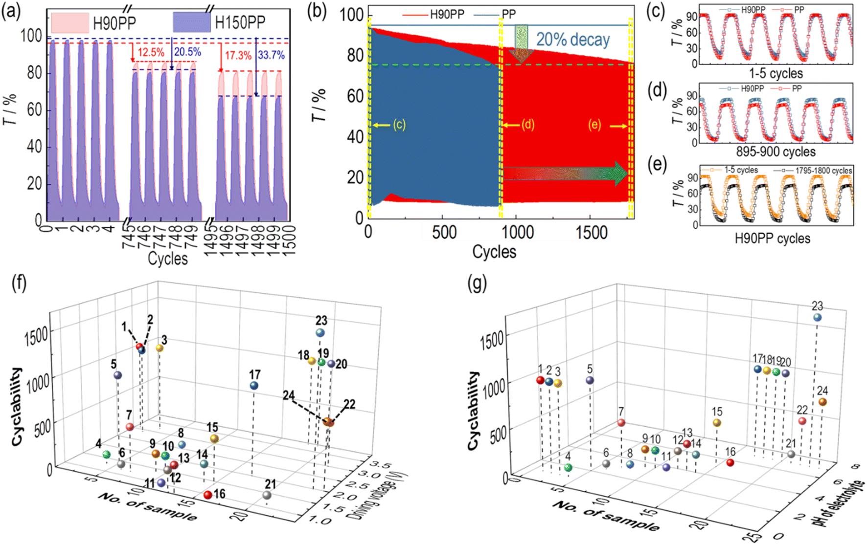 | ||
| Fig. 6 (a) The comparison of the cyclability of H90PP and H150PP for 1500 cycles; (b) the comparison of the lifetimes of PP and H90PP; the comparison of the EC performances for the first 5 cycles (c) and from the 895th to the 900th cycle (d) of H90PP and PP, which were extracted from Fig. 7b; (e) the comparison of the first 5 cycles and the last five cycles of the H90PP film. All the cycling measurements in this figure employed bare FTO as the background in a three-electrode system under the Eap of ±1.0 V using Ag/AgCl as the reference electrode, each potential step lasting for 10 s; (f) the comparison of the driving potential and cyclability with the literature; (g) the comparison of the pH of electrolyte and cyclability with the literature. The numbers in (f) and (g) are 1: TiO2 (NP)–P2W15V3; 2: TiO2 (NP)–P2W16V2; 3: TiO2 (NP)–P2W17V; 4: TiO2 (NP)–W10; 5: [P2W18/PAH/P2W18/TiO2]10; 6: (PDDA/W10)n (n = 3, 6, 10); 7: (PSS/PAH/Eu-P5W30/PAH)20; 8: [P2W18/PAH/P2W18/PEDOT]20; 9: PSS/Cu(phen)2/[(P2W17/Cu(phen)2)]30; 10: PSS/Fe(phen)3/[(P2W17/Fe(phen)3)]30; 11: PEI/[SiW9V3/PEI–Bi2O3]15/SiW9V3; 12: {[Ce(P2W17)2]/PAH}20; 13: PSS/PAH/(P2W15/PAH)20; 14: [P2W18/CS-CNTs]30; 15: PSS(PEI/PSS)3(PEI/W18O49)30/(PEI/P8W48)20; 16: nano-SnO2/PDDA/[PMo12O40]; 17: TiO2 (NP)–Na-P5W30; 18: TiO2 (NP)–PW11V; 19: TiO2 (NP)–PW10V2; 20: TiO2 (NP)–PW9V3; 21: {PEI/[P2W17V/PEI-CdS]30}P2W17V; 22: [PEI/P2W18/PEI/WO3]20; 23: H90PP (this work); 24: PP (this work). | ||
For the first five cycles, H90PP and H150PP showed similar ΔT values and response times. As the cycles increased to 800, T for H90PP and H150PP decreased in the bleached state, resulting in a decreased ΔT. H90PP showed a decrease of 12.5%, and H150PP showed a decrease of 20.5%. When the measurement was continued for up to 1600 cycles, H90PP and H150PP showed decreases of 17.3% and 33.7%, respectively. However, there were no obvious changes in the response time. There was a large difference in lifetime between H90PP and H150PP, which could be due to the large size of H150, which is 1.3 times larger than that of H90. For the octahedron-shaped HKUST particles, only one of the octahedron faces could be connected to the FTO substrate; thus, connection of larger sized particle like H150 may not be firm as small sized H90 particles. Therefore, the difference in cyclability between H90PP and H150PP could be attributed to the fact that H150PP may be partially detached from the FTO surface after a long cycle. Considering the cyclability and scattering effect, the optimized film should be H90PP.
The cyclability of H90PP and PP films was also measured under an Eap of ±1.0 V, as shown in Fig. 6b. The 20% decrease in optical contrast was employed to evaluate the cyclability. In general, the cyclability of the PP film and H90PP was 900 cycles and 1800 cycles, respectively, where the decrease of the optical contrast occurred due to the decrease of Tb. The colored state of the PP and H90PP films showed nearly no change over the cycles. The first 5 cycles are extracted in Fig. 6c, where the PP and H90PP film showed exactly the same EC performance as the very beginning. After 900 cycles, both PP and H90PP showed some decrease in ΔT (Fig. 6d) and ΔT decrease of the PP film already reached 20%. Nonetheless, their response times were the same as those of each other, even showing a more rapid response after the initial cycles of film activation. During the continued examination of the cyclability of H90PP, a gradual decrease in Tb was observed reaching 20% of the decrease after 1650 cycles. Compared with the first against the last five cycles of the H90PP (Fig. 6e), it can be seen that the response time and Tc remained constant even after 1650 cycles, while only the Tb loss was detected. This could be attributed to the Li+ cations, which diffused deeper into the PP film, making them difficult to deintercalate back under the same positive potential. The residual Li+ around P2W18 may hinder the film from achieving full bleaching after cycling. However, the introduction of porous HKUST particles could create many pores in the deep condensed part of the film, which shorten the ion diffusion pathway within the H90 particles and the interface between H90 and the film, resulting in prolonged cyclability for about 2 times. Finally, the Li+ cations diffused in the deeper part of PP between the H90 particles causing a loss of Tb. Therefore, the size of the HKUST-1 particles is not only relevant to ΔT and response times but also plays a crucial role in cyclability. Meanwhile, the Tc shows no change after 1650 cycles in the cyclability measurements of H90PP, which also indicates that there is no P2W18 loss from the film after cycling.
The cyclability of H90PP and PP was compared with the data from the literature, which is shown in Fig. 6f and g, Table S3.† The driving voltage and the pH of the electrolyte are taken into consideration to investigate the cyclability of POM-based films. The driving voltage is defined as the range of voltage for bleaching and coloration. The organic electrolyte (LiClO4 PC solution) was considered neutral (pH = 7). Samples 4 and 6 are W10 isopolyacid-based EC films, and their cyclability is within 100 cycles. Samples 11, 16, 18, 19, and 20 have a Keggin structure, while the others are Dawson and their derivative-based EC films with different preparation procedures, driving voltages and electrolytes, and their cyclability range was from 10 cycles to 1650 (this work) cycles, which indicated that the structure remains stable under reversible potential steps. In contrast, external factors like the film structure, driving potential, and electrolyte conditions determine the cyclability of POM-based films. As shown in Fig. 6f, a higher voltage may result in longer cyclability. When the driving voltage is lower than 2.0 V, the cyclability showed no more than 500 cycles. This means that under lower driving voltages, the intercalation and deintercalation of the cation cannot be fully achieved after cycling. The slight incomplete deintercalation of each cycle will accumulate after multiple cycles, which causes a decrease in cyclability. The higher applied voltage will realize the complete intercalation and deintercalation of the cations; however, the overpotential on the film might also cause the exfoliation of the film.36
The pH value of the electrolyte is another key factor in the stability of the POM-based EC films. Previously, it was widely accepted that the electrochemical activity of POMs can only be expressed at pHs of around 1 to 4; therefore, the buffer solution with pH around 2–4 was employed as the electrolyte (Table S3†). However, the acidic aqueous electrolyte was hard for further device preparation. Most of the POM films in LiClO4/PC showed higher cyclability than in acidic electrolyte, which could be due to the acidic solution that would cause film corrosion, resulting in exfoliation and film degradation. The superior cyclability was always found in the LiClO4/PC electrolyte system.
To fabricate the full cell ECD with energy storage properties (electrochromic energy storage device, EESD) based on H90PP, MnO2 was selected as the charge-balancing material on the CE. The EESD configuration is illustrated in Fig. 7a; using the 1.0 M LiClO4/PC solution as the electrolyte, the film is sealed within a PI tape spacer with a thickness of 100 μm between the WE and CE. The MnO2 films with different thicknesses (denoted as M5, M10, M15, and M20, respectively) were prepared using our previously reported method detailed in the ESI.† Fig. S14 and S15† show the transmittance and the thickness of the films. The CV curve of the MnO2 films at the scan rate of 10 mV s−1 was compared with that of H90PP in Fig. 7b. The M10 and M15 featured the closest areal current density with H90PP. However, taking the high transmittance into account, M10 is the optimized film as the charge balance CE for H90PP.
 | ||
| Fig. 7 (a) The illustration of the EESD configuration, showing a HnPP (n = 60, 90, 120, 150) layer between two pieces of FTO glass from the left to right, electrolyte layer: 1.0 M LiClO4/PC solution with a thickness of 50 μm, and a MnO2 layer with certain thickness; (b) the comparison of the CV curves of M10, H60PP, H90PP, H120PP and H150PP in 1.0 M LiClO4/PC solution at the scan rate of 100 mV s−1 in a three-electrode system; (c) the whole wavelength transmittance change of H90PP//M10 under different applied voltages in a two-electrode system in 1.0 M LiClO4/PC solution used as the electrolyte; (d) the transmittance changes of PP//M10 (solid lines) and H90PP//M10 (empty lines) under different Vap steps of 1: −0.5/1.0, 2: −0.8/1.0, 3: −1.0/1.0, 4: −1.2/1.2, 5: −1.5/1.5, and 6: −1.8/1.8 V, each step lasting for 10 s; (e) the GCD curve of the H90PP//M10 EESD under different current densities; negative electrode: H90PP electrode; positive electrode: M10 electrode; (f) the transmittance change (λ = 600 nm) along with the GCD process (0.1 mA cm−2) of H90PP//M10 EESD. | ||
The transmittance changes of the H90PP//M10-EESD under different applied voltages (Vaps) are shown in Fig. 7c. Compared to the H90PP film, the transmittance from 400 to 500 nm showed a decrease, which could be due to the absorbance of MnO2 on the CE. Both the pristine and the bleached H90PP//M10 devices showed a transmittance of 80% at 640 nm. As the Vap increased, the transmittance of the device decreased continuously. The maximum wavelength for optical modulation also shifted from 700 to 640 nm, which had the same shift tendency as the EC behavior of the PP film. The lowest transmittance of the colored state for the H90PP//M10 device was 10%, which was found at the wavelength of 640 nm under the Vap of −1.8 V.
The EC performance of PP//M10 and H90PP//M10 under different Vap steps is recorded in Fig. 7d. Under voltage steps of −0.5/1.0, −0.8/1.0, and −1.0/1.0 V, ΔT values of PP//M10 and H90PP//M10 were the same for both. The tc,90% value for H90PP//M10 was 1.0 s, 0.8, 0.8, 0.7, and 0.8 s under the voltage steps of −0.8/1.0, −1.0/1.0, −1.2/1.2, −1.5/1.5, and −1.8/1.8 V. However, tc,90% for PP//M10 was longer than that of H90PP//M10, i.e., 3.4, 2.2, 1.0, 1.4, and 2.2 s under −0.8/1.0, −1.0/1.0, −1.2/1.2, −1.5/1.5, and −1.8/1.8 V, respectively. The fast diffusion property and EC reactions in the H90PP films are retained in the full cell device configuration with MnO2 (ESI video 1†).
The CV curves of the H90PP//M10 EESD at different scan rates are shown in Fig. S16.† The characteristic peaks of P2W18 became less obvious due to the charge balance between H90PP and MnO2 in the device. The current density increased with the increase in scan rates, indicating good reversibility and a rapid redox reaction. The GCD curves in Fig. 7e showed the H90PP//M10-EESD maintaining the same shape at different scan rates, indicating a high reversible capacitance performance. The capacitance of the H90PP//M10 device was 7.89 mF cm−2 at a current density of 0.1 mA cm−2. The GCD process was accompanied by a significant change in transmittance ranging from 70% to 10% (Fig. 7f), which realized the visual evaluation of the energy level of the device.
The power density of the H90PP//M10-EESD was determined from areal capacity data. Since the thickness of the electroactive layer was quite thin, the areal capacity and calculated energy density were smaller than those of commercially available capacitors. However, as compared in Fig. 8a, the H90PP//M10-EESD exhibited higher values than most of the reported EESDs.40–46 When taking the optical contrast into consideration, H90PP//M10 showed the state-of-the-art performance among the reported similar types of EESDs40,41,43,46,47 (Fig. 8b). The cyclability of the H90PP//M10 EESD was measured under the voltage step of −1.8/1.8 V, and each potential step lasted for 10 s (Fig. 8c). The cyclability of the H90PP//M10 EESD was over 200 cycles. Different from the half-cell device (single electrode system), in the H90PP//M10 EESD, both the coloration and bleaching states showed some decrease in transmittance. There are possibly two reasons for this phenomenon. One is that in the H90PP film single electrode system, the Ag/AgCl electrode was employed as the reference electrode. Therefore, the applied potential on H90PP was precise as we set. However, in the device configuration, where there is no reference electrode, the applied voltage just equals the potential difference between the working electrode and counter electrode. Therefore, the actual voltage applied to the working electrode is unknown which might be different from the applied potential in the single electrode system. The other one is that the MnO2 film on the counter electrode forms a highly effective pseudocapacitive layer that significantly enhances charge storage by stabilizing ions through an electric double layer at the MnO2/electrolyte interface in EESDs. This phenomenon enhances the device's energy storage capacity. However, the stabilization of ions conflicts with the requirements for rapid ion movement necessary for the EC reaction, particularly during the coloration process. The ions that contribute to the formation of the stable double layer are not readily available for intercalation into or deintercalation from the electrochromic layer (eqn (1)–(3)), which results in the Tc as well as Tb decay after cycling. The 1.8 V voltage window of H90PP//M10-EESD was enough to power some low-voltage electronics, such as LED lights, electronic watches, etc. Considering the illumination of a red LED bulb as an example, upon connecting the LED to the charged H90PP//M10 EESD, the LED emitted a bright light until the EESD discharged to a residual voltage below 0.3 V. In Fig. 7f, the region of transmittance change, which corresponds to the energy-level variations of the EESD, is highlighted with a red background, to indicate the lighting of the LED bulb. A single H90PP//M10 EESD with an area of 2.0 cm2 is capable of providing visible emission to light the LED for approximately 60 seconds, as evidenced by the ESI video 2.† This illumination is accompanied by a noticeable color change of the H90PP//M10 EESD.
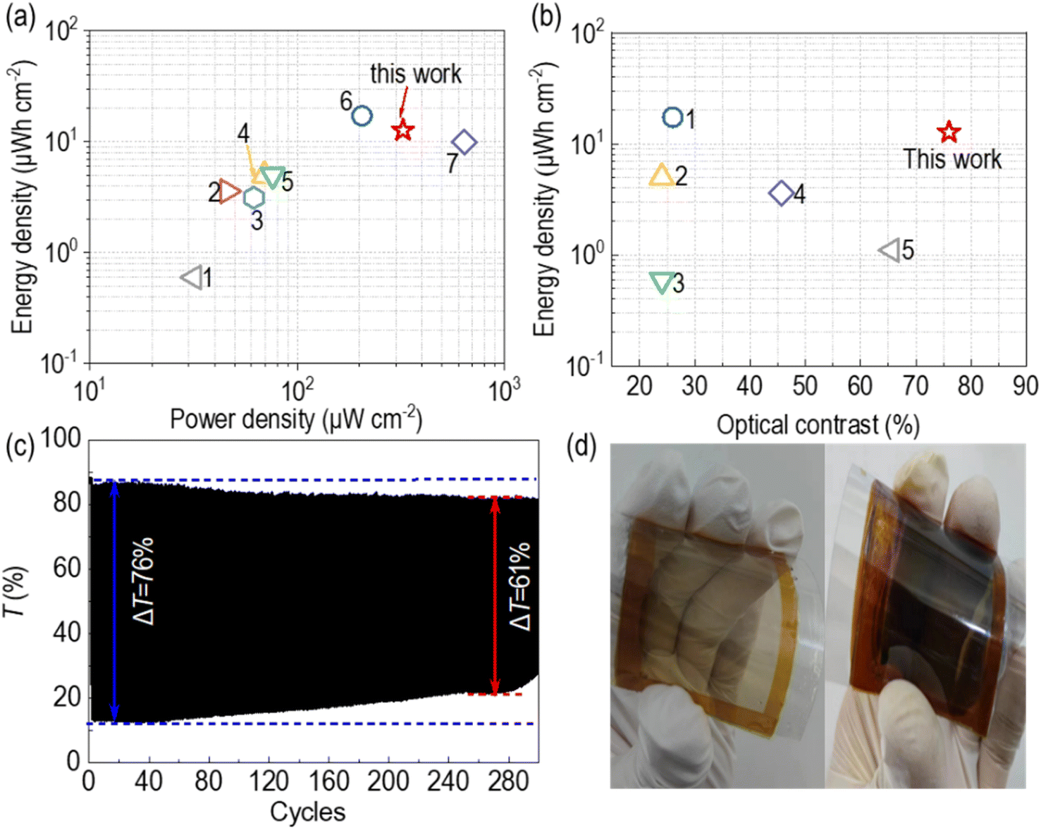 | ||
| Fig. 8 (a) Ragone plot of H90PP//M10 and reported similar inorganic EESDs using areal units, 1: WO3/Ag NWs/PEDOT:PSS‖WO3/Ag NWs/PEDOT:PSS; 2: WO3‖MoO3/Au/MoO3; 3: PANI‖PANI; 4: W0.71Mo0.29O3‖FTO; 5: poly(indole-6-carboxylic acid)‖poly(indole-6-carboxylic acid); 6: V2O5/MnO2‖FTO; 7: NiMoO4‖NiMoO4; this work: H90PP//M10; (b) comparison of the energy density and optical contrast of H90PP//M10 with reported inorganic EESDs, 1: V2O5/MnO2‖FTO; 2: W0.71Mo0.29O3‖FTO; 3: WO3/AgNWs/PEDOT:PSS‖WO3/AgNWs/PEDOT:PSS; 4: WO3‖MoO3/Au/MoO3; 5: WO3‖Prussian blue; this work: H90PP//M10; (c) the cycle stability of the H90PP//M10 EESD under the voltage step of −1.8/1.8 V, each Vap lasting for 10 s; (d) the images of the bleaching and colored flexible PP//M10 EESD under the Vap step of ±1.8 V, size: 8 × 8 cm2. | ||
Flexibility is very helpful for the practical application of ECDs. Previously, high-temperature processes or acidic conditions were needed for preparing the high-performance POM-based EC films (electrodeposition on porous TiO2 or the LBL method), which would cause the exfoliation of the conductive layer from the flexible substrate, limiting the development of the POM-based flexible devices. However, this spin-coating procedure for preparing the POM-based EC films, without any high temperature or acidic conditions, makes it possible to prepare films on the flexible ITO-PET substrate, opening up new possibilities for the POM-based flexible ECD. An 8 × 8 cm2 sized ITO-PET was employed as the substrate to illustrate the large-sized flexible device based on POMs. As shown in Fig. 8d, the PP//M10 flexible ECD showed a uniform color change under the Vap step of ±1.8 V. This is the first example for the flexible ECD based on POMs.
Conclusion
In conclusion, a P2W18–PVA (PP) based aqueous solution was developed that rehabilitates the facile spin coating method to make POM-based highly transparent and stable EC films. However, the slow electron transfer and ion diffusion rate in the condensed film of P2W18–PVA hindered the high EC performance of P2W18 and its cyclability. To address this issue, HKUST particles with different sizes were introduced to the film to improve the internal environment of the film. By imbedding the optimal-sized HKUST particles into the PP films, we achieved a larger interface area in the film with improved stability and EC electrochemical responses, resulting in full expression of the electrochemical activity and reversibility of the film similar to that of P2W18 itself. Furthermore, we observed significant differences in the ion diffusion and electron transfer pathways in the H90PP films compared to the PP film. As a result, the cyclability of the H90PP film was enhanced up to 1600 cycles, which showed a 2 times improvement compared to the PP film. When employing the MnO2 film as the CE, the full cell system of H90PP showed a high performance EESD with a capacity of 7.89 mF cm−2. Moreover, this PP solution was also suitable for spin coating to generate films on a flexible ITO-PET substrate. Thus, in this work, the first example of the flexible POM-based ECD was realized. This work not only developed a spin-coating method for POM-based EC films but also provided insights into enhancing the EC performance of spin-coated POM-PVA films through improvement in morphology. This spin-coating method would still show applicability for other soluble POMs.Data availability
The data supporting this article have been included as part of the ESI.†Author contributions
Shi-Ming Wang: supervision, conceptualization, writing – review & editing. Kai-Hua Wang: investigation, data curation, formal analysis, writing – original draft. Lu Zhou: investigation, software, validation. Tianyang Lu: software, validation. Eunkyoung Kim: writing – review & editing. Zhengbo Han: project administration. Jun Liang Lin: visualization, writing – review & editing. Lin Liu: software, writing – review & editing. Guodong Li: funding acquisition.Conflicts of interest
All authors declare no conflict of interest.Acknowledgements
We thank the Liaoning Province Science and Technology Department Program (2023JH1/10400056, 2023-MS-136, 2023JH2/101300007), the Scientific Research Foundation of the Department of Education of Liaoning Province (LJ212410140014, L242410140025), the National Natural Science Foundation of China (22171121), the China Scholarship council (202008210342), and the National Research Foundation of Korea (NRF) grant funded by the Korea government (MSIT) (No. RS-2023-00302697) for their support.References
- C. G. Granqvist, Sol. Energy Mater. Sol. Cells, 2000, 60, 201–262 CrossRef CAS.
- S. Cao, S. Zhang, T. Zhang, Q. Yao and J. Y. Lee, Joule, 2019, 3, 1152–1162 CrossRef CAS.
- R. K. Jain, A. Khanna, Y. K. Gautam and B. P. Singh, Appl. Surf. Sci., 2021, 536, 147804 CrossRef CAS.
- S. Liu, D. G. Kurth, H. Möhwald and D. Volkmer, Adv. Mater., 2002, 14, 225–228 CrossRef CAS.
- T. Ivanova, K. A. Gesheva, M. Ganchev and E. Tzvetkova, J. Mater. Sci.: Mater. Electron., 2003, 14, 755–756 CrossRef CAS.
- P. Jittiarporn, S. Badilescu, M. N. Al Sawafta, L. Sikong and V.-V. Truong, J. Sci.: Adv. Mater. Devices, 2017, 2, 286–300 Search PubMed.
- M. Han, C. H. Cho, H. Jang and E. Kim, J. Mater. Chem. A, 2021, 9, 16016–16027 RSC.
- J. Kim, D. Kim, H. Jang, Y. Auh, B. Kim and E. Kim, Chem. Eng. J., 2022, 450, 138081 CrossRef CAS.
- B. C. Thompson, Y.-G. Kim, T. D. McCarley and J. R. Reynolds, J. Am. Chem. Soc., 2006, 128, 12714–12725 CrossRef CAS.
- R. Li, X. Ma, J. Li, J. Cao, H. Gao, T. Li, X. Zhang, L. Wang, Q. Zhang, G. Wang, C. Hou, Y. Li, T. Palacios, Y. Lin, H. Wang and X. Ling, Nat. Commun., 2021, 12, 1587 Search PubMed.
- W. Zhang, H. Li, E. Hopmann and A. Y. Elezzabi, Nanophotonics, 2021, 10, 825–850 CAS.
- T. Buchecker, X. Le Goff, B. Naskar, A. Pfitzner, O. Diat and P. Bauduin, Chem.–Eur. J., 2017, 23, 8434–8442 CrossRef CAS.
- H. Jang, J. Kim, M. Han, C. Cho and E. Kim, J. Mater. Chem. A, 2023, 11, 3038–3050 RSC.
- S.-M. Wang, Y. Wang, T. Wang, Z. Han, C. Cho and E. Kim, Adv. Mater. Technol., 2020, 5, 2000326 CrossRef CAS.
- G. Decher, Science, 1997, 277, 1232–1237 CrossRef CAS.
- S.-M. Wang, L. Liu, W.-L. Chen, E.-B. Wang and Z.-M. Su, Dalton Trans., 2013, 42, 2691–2695 RSC.
- S. Takano, A. Kishimoto, K. Hinokuma and T. Kudo, Solid State Ionics, 1994, 70–71, 636–641 CrossRef CAS.
- T. He, Y. Ma, Y. Cao, W. Yang and J. Yao, J. Non-Cryst. Solids, 2003, 315, 7–12 CrossRef CAS.
- J. Kim, M. Rémond, D. Kim, H. Jang and E. Kim, Adv. Mater. Technol., 2020, 5, 1900890 CrossRef CAS.
- F. H. Falqi, O. A. Bin-Dahman, M. Hussain and M. A. Al-Harthi, Int. J. Polym. Sci., 2018, 2018, 8527693 Search PubMed.
- P. S. Premkumar, J. Mater. Res. Technol., 2019, 8, 2232–2237 CrossRef CAS.
- Y. Yang, J. Xu, Y. Li and G. Gao, J. Mater. Chem. C, 2019, 7, 12518–12522 RSC.
- K. H. Wu, P. Y. Yu, C. C. Yang, G. P. Wang and C. M. Chao, Polym. Degrad. Stab., 2009, 94, 1411–1418 CrossRef CAS PubMed.
- S.-M. Wang, J. Hwang and E. Kim, J. Mater. Chem. C, 2019, 7, 7828–7850 RSC.
- R. Li, K. Li, G. Wang, L. Li, Q. Zhang, J. Yan, Y. Chen, Q. Zhang, C. Hou, Y. Li and H. Wang, ACS Nano, 2018, 12, 3759–3768 CrossRef CAS PubMed.
- K. AlKaabi, C. R. Wade and M. Dincă, Chem, 2016, 1, 264–272 CAS.
- S.-M. Wang, Y. Kim, B. Kim, M. Han and E. Kim, Adv. Funct. Mater., 2019, 29, 1806590 CrossRef.
- Y.-S. Hsiao, C.-W. Chang-Jian, W.-L. Syu, S.-C. Yen, J.-H. Huang, H.-C. Weng, C.-Z. Lu and S.-C. Hsu, Appl. Surf. Sci., 2021, 542, 148498 CrossRef CAS.
- Q. Zhu, Y. Li, W. Wang, G. Sun, K. Yan and D. Wang, Compos. Commun., 2018, 10, 36–40 CrossRef.
- P. B. So, C.-Y. Liu, Y.-L. Lai, C.-S. Lee and C.-H. Lin, Mater. Adv., 2022, 3, 6458–6465 RSC.
- D. Mohanadas, N. I. A. Zainudin and Y. Sulaiman, Chem. Eng. J., 2022, 428, 130989 CrossRef CAS.
- A. Shameli and E. Ameri, Chem. Eng. J., 2017, 309, 381–396 CrossRef CAS.
- L. Liu, S.-M. Wang, C. Li, C.-G. Liu, C.-L. Ma and Z.-B. Han, J. Mater. Chem. C, 2015, 3, 5175–5182 RSC.
- S.-M. Wang, L. Liu, W.-L. Chen, Z.-M. Zhang, Z.-M. Su and E.-B. Wang, J. Mater. Chem. A, 2013, 1, 216–220 RSC.
- S. Liu, L. Xu, F. Li, W. Guo, Y. Xing and Z. Sun, Electrochim. Acta, 2011, 56, 8156–8162 CrossRef CAS.
- S.-M. Wang, Y.-H. Jin, L. Zhou, K.-H. Wang, H. J. Kim, L. Liu, E. Kim and Z. Han, ACS Appl. Mater. Interfaces, 2023, 15, 56242–56252 CrossRef CAS.
- J. L. Hauser, M. Tso, K. Fitchmun and S. R. J. Oliver, Cryst. Growth Des., 2019, 19, 2358–2365 CrossRef CAS.
- S.-M. Wang, L. Liu, W.-L. Chen and E.-B. Wang, Electrochim. Acta, 2013, 113, 240–247 CrossRef CAS.
- T. S. Mathis, N. Kurra, X. Wang, D. Pinto, P. Simon and Y. Gogotsi, Adv. Energy Mater., 2019, 9, 1902007 CrossRef CAS.
- F. Zhou, Z. Ren, Y. Zhao, X. Shen, A. Wang, Y. Y. Li, C. Surya and Y. Chai, ACS Nano, 2016, 10, 5900–5908 CrossRef CAS.
- H. Li, J. Li, C. Hou, D. Ho, Q. Zhang, Y. Li and H. Wang, Adv. Mater. Technol., 2017, 2, 1700047 CrossRef.
- H. S. Chavan, B. Hou, A. T. A. Ahmed, Y. Jo, S. Cho, J. Kim, S. M. Pawar, S. Cha, A. I. Inamdar, H. Im and H. Kim, Sol. Energy Mater. Sol. Cells, 2018, 185, 166–173 CrossRef CAS.
- Q. Liu, Z. Xu, W. Qiu, C. Hou, Y. Wang, P. Yao, R. Yu, W. Guo and X. Y. Liu, RSC Adv., 2018, 8, 18690–18697 RSC.
- Z. He, B. Gao, T. Li, J. Liao, B. Liu, X. Liu, C. Wang, Z. Feng and Z. Gu, ACS Sustainable Chem. Eng., 2019, 7, 1745–1752 CrossRef CAS.
- J. Li, Q. Guo, Y. Lu and G. Nie, Eur. Polym. J., 2019, 113, 29–35 CrossRef CAS.
- S. Sajitha, U. Aparna and B. Deb, Adv. Mater. Interfaces, 2019, 6, 1901038 CrossRef CAS.
- Z. Bi, X. Li, Y. Chen, X. He, X. Xu and X. Gao, ACS Appl. Mater. Interfaces, 2017, 9, 29872–29880 CrossRef CAS.
Footnote |
| † Electronic supplementary information (ESI) available. See DOI: https://doi.org/10.1039/d4ta06915c |
| This journal is © The Royal Society of Chemistry 2025 |