
Magic guanidinium cations in perovskite solar cells: from bulk to interface
Pengfei
Wu
ab,
Dewang
Li
*cd,
Shirong
Wang
 *ab and
Fei
Zhang
*ab
*ab and
Fei
Zhang
*ab
aSchool of Chemical Engineering and Technology, Tianjin University, Tianjin 300072, China. E-mail: wangshirong@tju.edu.cn; fei_zhang@tju.edu.cn
bCollaborative Innovation Center of Chemical Science and Engineering (Tianjin), Tianjin 300072, China
cInternational Campus of Tianjin University, Joint School of National University of Singapore and Tianjin University, Fuzhou 350207, China. E-mail: lidewang@tju.edu.cn
dSchool of Materials, Science and Engineering Tianjin Key Laboratory of Composite and Functional Materials, Tianjin University, Tianjin 300350, China
First published on 6th March 2023
Abstract
Guanidinium (GA+) has been proven as the multifunctional cation in halide perovskite solar cells (PSCs), attracting considerable attention due to its improved power conversion efficiencies (PCE) and operational stability. This review introduces the elementary properties of the GA cation and GA-based perovskite. Then, we summarize the development history of utilizing guanidinium materials in PSCs, including composition engineering, additive engineering, and interface engineering, accompanied by their optimization mechanisms. Moreover, we propose a perspective on the potential opportunities in this popular field and challenges to the future design of guanidinium-based PSCs with enhanced performance.
 Pengfei Wu | Pengfei Wu is currently a PhD candidate in Applied Chemistry at Tianjin University under the supervision of Prof. Shirong Wang. He received his BS degree (2019) from China University of Petroleum (East China), China. His current research focuses on low-dimensional perovskites and efficient perovskite solar cells. |
 Dewang Li | Dewang Li received his Master's degree in Materials Science and Engineering and PhD degree in Chemical Engineering and Technology from Tianjin University in 2016 and 2021, respectively. He is currently a postdoctoral fellow in the Joint School of National University of Singapore and Tianjin University (Fuzhou, China). His research interests focus on perovskite solar cells, quantum dot light-emitting diodes, and next generation metal–air batteries. |
 Shirong Wang | Shirong Wang is currently a Professor in the School of Chemical Engineering and Technology at Tianjin University. She received her BS degree (1991) and PhD degree in Applied Chemistry at Tianjin University. She worked as a postdoctoral researcher in the State Key Laboratory of Fine Chemicals at the Dalian University of Technology. Her main research interests include perovskite solar cells, organic/quantum dots, light-emitting diodes, and metal halide perovskite nanocrystals. |
 Fei Zhang | Fei Zhang is currently a Professor in the School of Chemical Engineering and Technology at Tianjin University. He received his BEng (2011) and PhD degree (2017) under the supervision of Prof. Shirong Wang at Tianjin University. He was a visiting PhD student in LPI at Ecole Polytechnique Fédérale de Lausanne (EPFL) under the supervision of Prof. Michael Grätzel and Dr Shaik Mohammed Zakeeruddin. Then, he worked as a Postdoctoral Researcher in the Chemistry and Nanoscience Center at the National Renewable Energy Laboratory under Dr Kai Zhu's supervision. His interests concentrate on synthesizing low-dimensional perovskites, lead-free perovskites, and device engineering for perovskite optoelectrical devices. |
1. Introduction
To deal with the issues of energy crisis and greenhouse effect-induced climate change, it is essential to exploit renewable energy technologies, in which photovoltaics (PV) has been one of the most promising candidates to generate inexhaustible and clean solar energy. Among the various PV technologies, halide perovskite solar cells (PSCs) have attracted extensive interest due to their efficient power conversion efficiency (PCE), high voltage output, low fabrication cost, and simple processing techniques.1–3 The optimization strategies towards perovskite solar cell devices such as composition engineering, additive engineering, and interface engineering help advance the performance improvements, which recently reached over 25% for typical FAPbI3 PSCs.4,5 Nevertheless, the scalability and stability of such composition remain an issue because of the defects at the interfaces and grain boundaries and intrinsic phase segregation with ion migration.6–8To overcome the abovementioned drawbacks, bulky or long-chain organic cations such as butylammonium (C4H9NH3+ [BA+]), phenethylammonium (C8H9NH3+ [PEA+]), and octylammonium (CH3(CH2)7NH3+ [OA+]) could be introduced to passivate the various trap states and enhance the stability of the perovskite.9–11 These cations demonstrate significantly improved operational stability under multiple environments (e.g., moisture, thermal, and illumination). Unfortunately, their positive effects on the photovoltaic performance are not satisfying and are primarily limited by the hindered carrier transport because of the relatively low conductivity.12,13 Additionally, these cations hardly form and diffuse into the 3D perovskite crystal structure due to the large ionic radius.
Among various kinds of cations, GA+ is substantially larger in ionic radius (278 pm) as compared to the commonly used MA+ (217 pm) and FA+ (253 pm) cations while smaller than BA+ (393 pm) and PEA+ (437 pm). Still, it does not form a 3D perovskite structure as the sole A-cation in terms of the t value (see detailed information in Table 1).14,15 Regardless of the phase of the GA+-containing perovskites, positive interactions are usually found endowed by GA+, as long as it could be introduced in the system. GA has nearly zero dipole character, which has been proven to be effective in suppressing bias-induced ionic mobility and hysteresis characteristics.16,17 In addition, GA+ can offer a lone pair of electrons to specifically passivate the imperfections in the surface and bulk perovskite films, i.e., ionic vacancies, uncoordinated Pb, and/or Pb clusters.18 Most importantly, owing to the plentiful ammonium groups in the molecular structure, GA+ could provide more hydrogen bonds to coordinate with the surrounding halides, especially undercoordinated I− ions firmly, thus increasing the formation energy of halide vacancies and improving the perovskite structural stability.19,20 As a consequence, the charge carrier lifetime and photovoltaic performance, such as the cell's open circuit voltage (VOC) and fill factor (FF) are expected to be ameliorated.
| A-site cations | Formula | Radius (pm) | t | μ e (Debye) |
|---|---|---|---|---|
| Note: the t is calculated based on the chemical formula APbI3; the ionic radius of Pb and I are 220 pm and 119 pm, respectively. “—” means the absence of relative information elsewhere. | ||||
| Potassium | K+ | 137 | 0.74 | 10.82 |
| Ammonium | [NH4]+ | 146 | 0.76 | 0 |
| Rubidium | Rb+ | 152 | 0.78 | 11.48 |
| Cesium | Cs+ | 167 | 0.84 | 11.69 |
| Methylammonium | [(CH3)NH3]+ | 217 | 0.91 | 2.17 |
| Azetidinium | [(CH2)3NH2]+ | 250 | 0.98 | 2.51 |
| Formamidinium | [NH2(CH)NH2]+ | 253 | 0.99 | 0.60 |
| Dimethylammonium | [(CH3)2NH2] + | 272 | 1.02 | 1.80 |
| Ethylammonium | [(C2H5)NH3]+ | 274 | 1.03 | 4.49 |
| Guanidinium | [C(NH2)3]+ | 278 | 1.04 | 0 |
| Tetramethylammonium | [(CH3)4N]+ | 292 | 1.07 | 0 |
| Ethylenediammonium | [NH3(CH2)2NH3]22+ | 333 | 1.15 | — |
| Butylammonium | [(C4H9)NH3]+ | 393 | 1.28 | — |
| Phenylethylammonium | [C2H4(C6H5)NH3]+ | 431 | 1.35 | 1.5 |
| Butane-1,4-diammonium | [NH3(CH2)4NH3]22+ | 457 | 1.41 | — |
| Hexane-1,6-diammonium | [NH3(CH2)6NH3]22+ | 582 | 1.67 | — |
The GA cation-based material was first introduced in the dye/liquid electrolyte interface as an additive by Jeanbourquin et al.24 to improve the performance of dye-sensitized solar cells (DSSCs) in 2014. The additive could eliminate the interfacial dye–I2 complexes, increasing the collection efficiency and thus the photocurrent. Inspired by this, in 2016, Marco et al.25 also added the GA-based additive firstly into the perovskite precursor to suppress nonradiative recombination defects of iodide vacancies in the bulk and iodine species at grain boundaries, resulting in superior performance with PCEs of more than 17% and a minor VOC loss of 0.43 eV. Encouraged by the progress, GA-based materials seemed to be good candidates for PSCs, which have acquired rapid development in the past few years. In this passage, representative endeavors on the GA+ species for PSC developments have been summarized, which could be categorized into three strategies of compositional engineering, additive engineering, and interface engineering, among which the first one could be further classified into 3D compositional or 2D alternating-cation-interlayer (ACI) engineering types according to the perovskite matrix (Fig. 1). Although there have been reports of further PCE performances of over 24%, their simultaneous long-term stabilities against thermal, illumination or other harsh conditions have yet to be presented.20,26 Therefore, how to simultaneously achieve both excellent efficiency and stability of the device would be the significant challenge in the future for GA-based PSCs. This systematic review could help us identify the fundamental mechanisms and the origins of the existing problems. Conversely, it further opens access to rational designs to overcome the challenges and fabricate more stable and efficient PSCs.
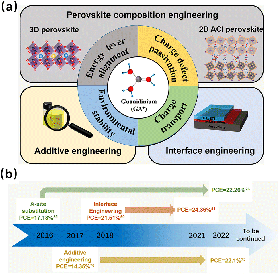 | ||
| Fig. 1 (a) The schematic diagram of strategies for the GA+ cation in the PSCs. (b) The development of GA+-based PSCs. | ||
2. Structure and optical properties
Metal halide perovskites may crystallize into zero-dimensional (0D), 1D, 2D, or 3D perovskite structures, as shown in Fig. 2. The tolerance factor (t) defines the geometrical criteria for the formation of an ideal cubic perovskite structure:where RA, RB, and RX are the ionic radii for the corresponding ions of cations in A sites, metals in B sites, and halides in X sites, respectively.

 | ||
| Fig. 2 Schematic representation of the halide perovskite with different dimensionalities from 3D to 0D at the structural level (top) and by morphology (bottom). | ||
When t is in the range of ∼0.8–1.0, a stable 3D perovskite structure can be formed. The 2D perovskite is preferred for inclusion in the case of t > 1,27 which generally adapts a formula of (A′)m(A)n−1BnX3n+1. Here, A′ is structurally featured with divalent (m = 1) or monovalent (m = 2) cations, and n indicates the number of layers consisting of [BX6]4− octahedra. 1D perovskite micro/nanocrystals generally present a well-defined fiber or ribbon-like morphology. Distinct from the uniform 3D growth, the self-assembly of the precursors into a 1D nanostructure reacting in a particular solution or vapor environment, as well as the ordered texture aligned by external forces such as casting and evaporation techniques or the periodically confined nano-templates, consists of the two prerequisites for practical 1D perovskite applications.28 0D perovskites have the formula 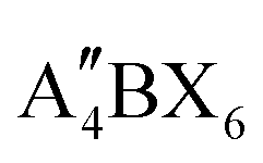 consisting of A′′—a monovalent organic or inorganic cation, and isolated BX6 octahedral anions or separated clusters from each other by the surrounding inorganic or organic cations without certain composition and periodic bands' formation. Therefore, the t of 0D perovskite often deviates from 1.29
Within the 3D framework, the inorganic layers of the [BX6]4− octahedra are connected via sharing each of their six corners, while the A cations occupy voids between each layer.30 In the case of B and X, respectively, representing pure Pb2+ and I−, the notorious B site oxidation and phase segregation problem can be avoided. When the A site is Cs+, MA+, FA+, and their alloys, t falls typically in the range of 0.8–1, which ensures a 3D cubic/tetragonal structure. Compared to cations with moderate radii in the 3D perovskites, the A-site in a 2D perovskite occupied by large radii organic cations such as PEA+ and BA+ would result in t > 1. They cannot fit into the voids between the octahedral units. After insertion, the A-site cations expand the van der Waals gaps, making the inorganic layers discrete, along with the broadened band gaps.31
Different from MA+ and FA+, GA+ is highly symmetric and non-polarized, and the lattice can be stabilized by its abundant hydrogen bonds. However, because of the large cation radii leading to the high lattice stress, the 3D [PbI6]4− octahedra networks break into the 1D ribbon (Fig. 3a) of the GAPbI3 form with edge-sharing octahedra or GA2PbI4, which is a 2D layer structure (Fig. 3b) with corner-sharing octahedra.32 The crystallographic data of GAPbI3 and GA2PbI4 are summarized, as shown in Fig. 3c and d, and Table 2. In the GA–Pb–I system, GA in the unit cell is approximately orientated along the (11![[1 with combining macron]](https://www.rsc.org/images/entities/char_0031_0304.gif) ) plane and connects with six I ions to generate N–H⋯I hydrogen bonds within the PbI6 octahedra, in the most stable structure. Furthermore, compared to MAPbI3 and FAPbI3 perovskites, the GA-based perovskite has more N–H⋯I hydrogen bonds in the unit cell (the number of N–H⋯I hydrogen bonds in MAPbI3, FAPbI3, and GAPbI3 are 3, 4, and 6, respectively) (Fig. 3e).33 Different conditions could regulate the formation of diverse dimensional GA–Pb–I perovskites. A solution process, such as spin-coating, is expected to deposit the 1D GAPbI3 and 2D GA2PbI4 perovskite film with a stoichiometric ratio of PbI2 and GAI.
) plane and connects with six I ions to generate N–H⋯I hydrogen bonds within the PbI6 octahedra, in the most stable structure. Furthermore, compared to MAPbI3 and FAPbI3 perovskites, the GA-based perovskite has more N–H⋯I hydrogen bonds in the unit cell (the number of N–H⋯I hydrogen bonds in MAPbI3, FAPbI3, and GAPbI3 are 3, 4, and 6, respectively) (Fig. 3e).33 Different conditions could regulate the formation of diverse dimensional GA–Pb–I perovskites. A solution process, such as spin-coating, is expected to deposit the 1D GAPbI3 and 2D GA2PbI4 perovskite film with a stoichiometric ratio of PbI2 and GAI.
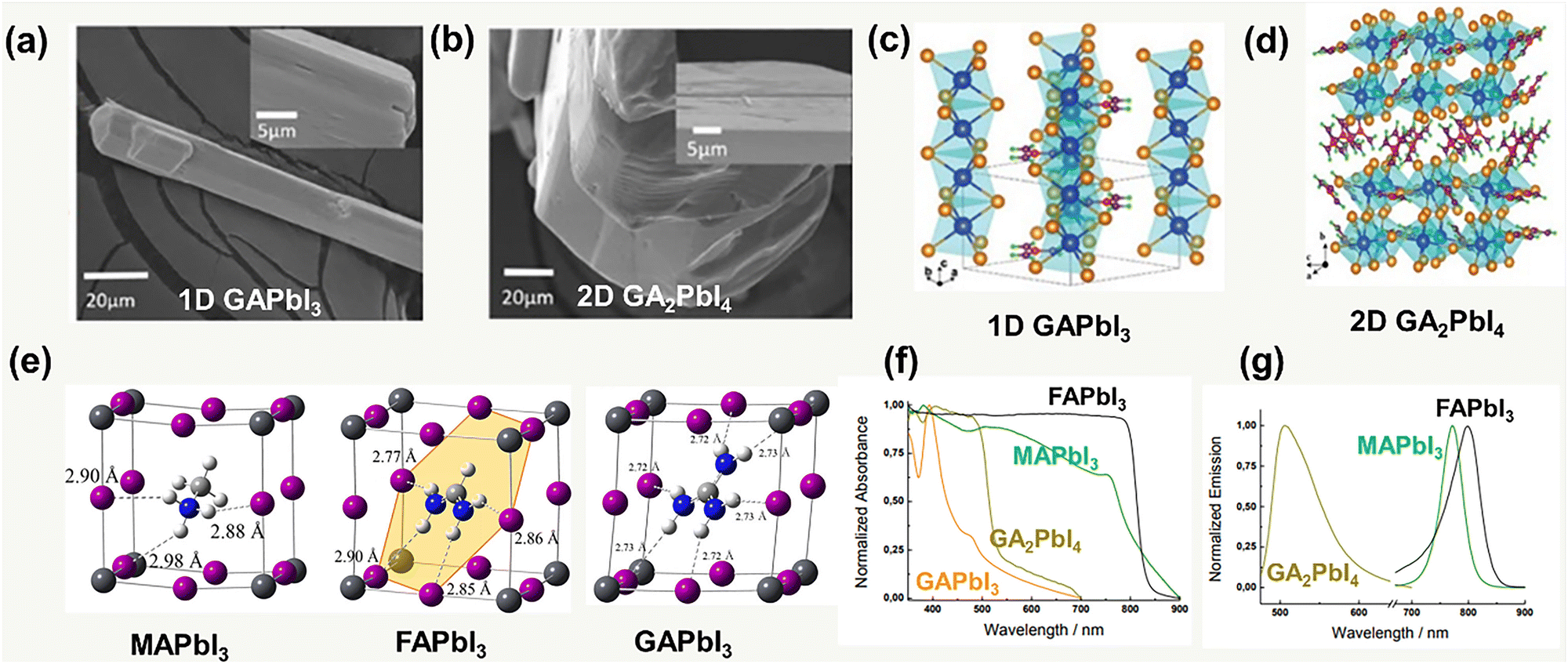 | ||
| Fig. 3 SEM images of (a) GAPbI3 and (b) GA2PbI4 (high-resolution SEM image as inset). Crystal structure of (c) 1D GAPbI3 and (d) 2D GA2PbI4. Reproduced with permission.32 Copyright 2021, ACS Publishing Group. (e) PbI6 inorganic framework and N–H⋯I hydrogen bonds in MAPbI3, FAPbI3, and GAPbI3. Reproduced with permission.33 Copyright 2018, ACS Publishing Group. (f) UV-vis absorption and (g) steady-state photoluminescence spectra of MAPbI3, FAPbI3, GAPbI3, and GA2PbI4. Reproduced with permission.36 Copyright 2016, Wiley-VCH. | ||
| Chemical formula | GAPbI3 | GA2PbI4 |
|---|---|---|
| Formula weight | 641.93 | 834.97 |
| Crystal system | Monoclinic | Orthorhombic |
| Space group | Pnma | P21/n |
| a (Å) | 11.9866(5) | 9.2440(3) |
| b (Å) | 4.4740(2) | 26.9511(11) |
| c (Å) | 20.8652(10) | 12.7155(3) |
| α (deg) | 90 | 90 |
| β (deg) | 90 | 91.482(2) |
| γ (deg) | 90 | 90 |
| Volume (Å3) | 1118.96(9) | 3166.82(17) |
| Z | 4 | 8 |
| ρ calc (g cm−3) | 3.81 | 3.503 |
The photophysical property of the GA-based perovskite, in contrast to MAPbI3 and FAPbI3, has an apparent blue shift of the absorption, which is also ascribed to the disruption of the coherent 3D PbI6 octahedra by the large size of the GA cation.34 Thereby, GA-based perovskite, for example, GAPbI3, provides a higher band gap (Eg) of 2.25 eV.35 The photoluminescence spectra of both GAPbI3 and GA2PbI4 also show the apparent shifts toward higher energy, which is in agreement with the results of the absorption spectra36 (Fig. 3f and g). Due to the wide bandgap, the GA-based perovskite could not generate a sufficient visible light-induced carrier. Moreover, GAPbI3 and GA2PbI4 usually exhibit poor uniformity in film processing, which makes them ineffective for direct use as photoactive layers in PSCs. However, it would become effective in the case of GA as a supplementary composition, as introduced by the above-mentioned three strategies in Fig. 1.
3. Composition engineering
Perovskite compositional engineering could improve the PCE and stability of the PSCs. Until now, the commonly used perovskite composition has been changed from the initial MAPbI3 to the so-called triple cation (MAxFA1−x)m Cs1−mPb(I1−yBry)3 perovskite, which recently illustrated a comparable development in PCE to the record. Although it has a large radius, GA+ could also be partially introduced into the A-site, which brings more lattice stability, bulk defect passivation from lone-pair electrons and hydrogen bonds, band structure adjustment, among other properties. The alloying could drastically improve the charge extraction and transport, and resistance against harsh conditions, resulting in enhanced device performance and stabilities.38,39 According to the dimension, the composition engineering will be divided into 3D perovskite composition engineering and 2D ACI composition engineering, whose PCEs have reached as high as 22.17% and 22.26%, respectively.3.1 3D perovskite composition engineering
Although the MA-and FA-based PSCs commonly exhibit excellent PCEs, MA and FA cations suffer from the degradation of perovskite film under light and thermal exposure due to the low stability of the perovskite film and phase impurity.40,41 Generally, the incorporation of GA, similar to Rb and Cs, could stabilize the perovskite phase, leading to enhanced performance and stability.41,42Besides the improved photovoltaic performance, the long-time thermal and photo instabilities are also of vital concerns. Jodlowski et al.43 incorporated the GA+ into the MAPbI3 perovskite film, forming the stable 3D perovskite structure. The SEM results showed that when x < 25%, the grain size was increased without unwanted phase segregation, whereas higher amounts of GA+ (x > 25%) tended to form the 1D GAPbI3 perovskite (Fig. 4a and b). Besides the improved film quality, the employed GA+ offered more H bonds within the inorganic framework to stabilize the 3D perovskite structure, resulting in improved efficiency and resistance to thermal and light corrosion.
 | ||
| Fig. 4 (a) Normalized XRD patterns of perovskite films with different amounts of GA. (b) Top-view SEM images of MA1−xGAxPbI3 with x = 0, 0.14, 0.30, and pure GAPbI3. Reproduced with permission.43 Copyright 2017, Nature Publishing Group. (c) XRD data for perovskite films with different GAI doping. Reproduced with permission.44 Copyright 2022, Wiley-VCH. (d) Schematic illustration of the halide ion distribution in the GAxCs1−xPbIBr2 lattice in response to a low-power laser (1.27 mW). (e) Normalized PCEs of CsPbIBr2- and GA0.1Cs0.9PbIBr2-based PSCs under continuous illumination for 8 h with the AM 1.5G solar spectrum in the ambient environment (∼55% relative humidity) without encapsulation. Reproduced with permission.45 Copyright 2022, Wiley-VCH. | ||
Moreover, GA+ has a significant effect on the inhibition of ion migration, which is responsible for the hysteresis and poor stability of the device.48,49 Ferdani et al.50 reported that MAPbI3 with 5% GA+ substitutions had higher activation energy (Ea = 0.78 eV) for iodide ion conduction than that of pristine MAPbI3 (Ea = 0.44 eV). Furthermore, Minussit et al.49 found that GA+ could slow down the relaxation process of space charge, which was two orders of magnitude longer, resulting in retarded ion migration. Meanwhile, incorporating GA+ has an impact on the low-temperature phase transitions of MAPbI3. When MA was substituted by 2 mol% GA+, the β (tetragonal) to α (cubic) phase transition happened under a reduced temperature of 278 K.
Wang et al.44 added GAI in the triple halide-mixed CsPbTh (Th = either I, Br, or Cl). The GA composition guaranteed the stabilization of the crystal lattice, achieving enhanced thermal stability (Fig. 4c). After that, the optimal device was obtained by PbAc2 introduction as a nucleating additive, accompanied with GCA spin-coated for interface passivation. Eventually, it delivered a PCE of 19.37% with a high FF of 82.7% and VOC of 1.17 V, and the operational stability was also dramatically improved. A more profound mechanism of the I− ion migration suppression was proposed, suggesting that the strengthened hydrogen bonds between the GA+ and the [PbI6]4− octahedron were responsible for reducing the local lattice distortion, which was the origin of ion migration45 (Fig. 4d). The retardation of light-induced ion migration via GA+ incorporation could retain over 80% under 8 h continuous illumination, showing superior light stability to the pristine CsPbIBr2 (Fig. 4e).
Hysteresis has raised the concern of accurate performance measurement in practice, while its origin remains an open question. GA+ participation could inhibit hysteresis, with diverse interpretations of the mechanisms. Wang et al.53 added GAI in a FA/Cs-based perovskite to regulate the energy alignment and extend the PL lifetime. Consequently, the low content of GA+ in the FA/Cs-based perovskite induced a slight lattice expansion, but could reduce interfacial charge accumulation, thus removing the J–V hysteresis while improving PCE (Fig. 5a and b). On the other hand, Li et al.54 explored the MA0.8FA0.1GA0.1PbI3 system, and concluded that the GA+ incorporation into the perovskite structure could build the potential barrier of iodide ion migration and improve the perovskite crystalline, achieving the best PCE of over 22% and 19.18% for an active area of 14 cm2 (Fig. 5d and e).
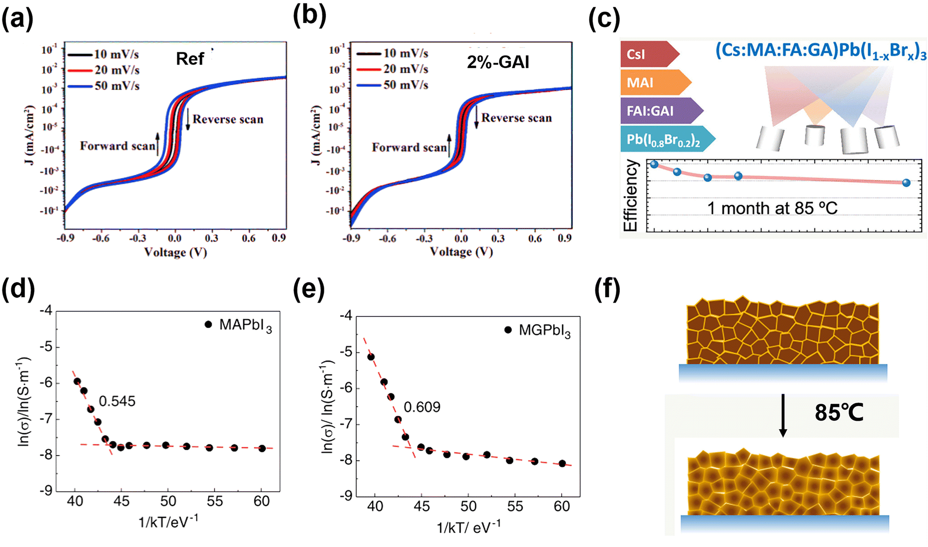 | ||
| Fig. 5 Dark J–V curves in logarithm scaled current representation at different scan rates for (a) the control device and (b) the device with 2% GAI. Reproduced with permission.53 Copyright 2019, Wiley-VCH. Temperature-dependent ion conductivity of the (d) MAPbI3 (control) and (e) MA0.9GA0.1PbI3 (MGPbI3). Reproduced with permission.54 Copyright 2022, Wiley-VCH. (c) J–V curves of quadruple-cation CsMAFAGA-based device at 85 °C. (f) Schematics of GA+ dynamic incorporation in vacuum-deposited, quadruple cation CsMAFAGA perovskite films. Reproduced with permission.55 Copyright 2022, ACS Publishing Group. | ||
Due to the limited number of thermal sources and complexity of the Cs/MA/FA triple-cation-based perovskite, it is difficult to insert the GA+ into the lattice to form the CsMAFAGA quadruple-cation perovskite via solution process and conventional vacuum process. However, Susic et al.55 realized the uniform alloying by sublimation of FA and GA in the same thermal source during vacuum deposition, given that the sublimation properties of FAI and GAI were similar. The GA+ initially accumulated at the grain boundaries. However, upon subsequent annealing, it progressively penetrated the crystal and induced a lower-symmetry phase perovskite structural change to relieve the strain stress. Ultimately, stabilization of the cubic phase with a larger unit cell volume was observed (Fig. 5c and f). The CsMAFAGA-based device could maintain the perovskite structure, and no parasitic phase (PbI2, δ-CsPbI3, and δ-FAPbI3) formed at 85 °C after 37 days, demonstrating no degradation or segregation after stabilization by GA cations. Simultaneously, it kept over 75% original PCE at the 85 °C for about a month.
Although the GA+ in A-site compositional engineering plays an important role in the double-, triple- and even multiple-cation-based perovskite system for the ion migration inhibition, perovskite structure stabilization, charge defects passivation, and band structure change, it inevitably increases the complexity of the perovskite system for processing. In addition, introducing a high concentration of GA+ (more than 20%) could facilitate low-dimensional perovskite impurities, such as 1D GAPbI3 and 2D GA2PbI4 rather than uniform alloying in 3D structure, which would be imperfections in the interface and grain boundaries. The limited doping concentration becomes the bottleneck in composition engineering, so other guanidinium-involving approaches for perovskite modification would be the alternative for performance enhancement.
3.2 2D ACI composition engineering
Similar to the 2D Ruddlesden–Popper (RP) and Dion–Jacobson (DJ) perovskite, the GA-based 2D perovskites usually present excellent hydrophobicity and ambient stability. RP and DJ have the same chemical formula of . Here, A′ is structurally featured with bulky or long-chain monovalent organic cations for the 2D RP-perovskite, while divalent interlayer organic cations are suitable for the 2D DJ-perovskite. Unfortunately, the expanded interspaces filled with such bulky organic cations result in increased exciton binding energy and charge transfer barriers between the inorganic parts. The enlarged bandgap also brings the loss of optical absorption. Theoretically, it is hard to achieve a satisfying photovoltaic performance in the case of the normal 2D perovskite as a photoactive layer. Thus, partially replacing GA with a smaller molecule, forming the 2D ACI perovskite with a narrower band gap, has drawn considerable attention. 2D ACI follows the formula (A′)(A)nBnX3n+1, where the slightly larger A′ cation (e.g., GA+) and smaller A cation (e.g., MA+) form an alternating arrangement in the interlayer space. So far, Cs, MA, FA, and otheres are typically regarded as the substitutable spacer to build 2D ACI perovskites together with GA cations. The crystallographic data of the ACI perovskites reported are presented in Table 3.
| GAMAPbI4 | GAMA2Pb2I7 | GAMA3Pb3I10 | GACsPbI4 | GACsPbBr4 | GACs2Pb2Br7 | GAFAPbI4 | |
|---|---|---|---|---|---|---|---|
| Formula wt | 807.0 | 1426.9 | 2046.9 | 907.79 | 719.83 | 1299.66 | 819.95 |
| Temperature (K) | 293 | 300 | 298 | ||||
| Color | Yellow | Dark red | Black | Red | Yellow | Yellow | Brown |
| Morphology | Plate | None | None | None | Platelet | ||
| Crystal system | Orthorhombic | Monoclinic | |||||
| Space group | Imma | Bmm2 | Imma | Pnnm | Imma | Cmmm | C2/m |
| Volume (Å3) | 1507.7(2) | 2508.2(3) | 3473.8(5) | 2897.3(5) | 1226.2(2) | 2003.2(7) | 4678.7(7) |
| Unit cell dimensions (Å) | a = 6.4286(6) | a = 6.3729(4) | a = 6.3520(7) | a = 12.7426(13) | a = 6.0613(6) | a = 6.0029(12) | a = 26.948(2) |
| b = 12.4577(9) | b = 12.5435(8) | b = 12.4378(9) | b = 8.5776(19) | b = 11.5868(12) | b = 28.773(6) | b = 12.8189(11) | |
| c = 18.8258(13) | c =31.376(2) | c = 43.970(3) | c = 12.2390(13) | c = 17.4591(18) | c = 11.598(2) | c = 14.4080(12) | |
| Z | 4 | 8 | 4 | 4 | 12 | ||
| ρ calc (g cm−3) | 3.5551 | 3.7788 | 3.9138 | 4.162 | 3.899 | 4.309 | 3.492 |
| μ (mm−1) | 19.349 | 22.017 | 23.395 | 22.607 | 29.671 | 34.311 | 18.710 |
| F(000) | 1392 | 2424 | 3464 | 3056 | 1240 | 2208 | 4224 |
| Crystal size (mm3) | 0.1111 × 0.0225 × 0.0167 | 0.0511 × 0.179× 0.0100 | 0.0733 × 0.0372× 0.0193 | 0.3 × 0.07 × 0.02 | 0.2 × 0.08 × 0.02 | 0.46 × 0.08 × 0.04 | 0.32 × 0.06 × 0.04 |
| θ range (deg) | 3.27–29.23 | 2.6–29.27 | 2.78–29.29 | 3.876–63.122 | 4.218–62.904 | 3.512–62.718 | 3.006–52.738 |
| Index ranges | −8 ≤ h ≤8 | −8 ≤ h ≤8 | −8 ≤ h ≤ 8 | −18 ≤ h ≤ 17 | −8 ≤ h ≤ 8 | −8 ≤ h ≤ 8 | −33 ≤ h ≤ 33 |
| −17 ≤ k ≤ 16 | −17 ≤ k ≤ 17 | −17 ≤ k ≤ 16 | −26≤ k ≤ 26 | −17 ≤ k ≤ 16 | −41 ≤ k ≤ 41 | −16 ≤ k ≤ 16 | |
| −25 ≤ l ≤ 25 | −42 ≤ l ≤ 42 | −57 ≤ l ≤ 60 | −17 ≤ l ≤ 17 | −25 ≤ l ≤ 24 | −16 ≤ l ≤ 16 | −18 ≤ l ≤ 18 | |
| Reflections collected | 7172 | 11![[thin space (1/6-em)]](https://www.rsc.org/images/entities/char_2009.gif) 855 855 |
12119 |
33586 |
7142 | 11917 |
21674 |
| Independent reflections | 784 [Rint = 0.1277] | 2595 [Rint = 0.0563] | 1810 [Rint = 0.1261] | 4767 [Rint = 0.0637, Rσ = 0.0432] | 1094 [Rint = 0.0406, Rσ = 0.0295] | 1814 [Rint = 0.0473, Rσ = 0.0370] | 5009 [Rint = 0.0386, Rσ = 0.0319] |
| Completeness to θ | 99% | 99% | 99% | None | None | None | None |
| Data/restraints/parameters | 784/3/2 | 2595/9/82 | 1810/5/59 | 4767/18/109 | 1094/0/40 | 1814/0/58 | 5009/0/144 |
| Goodness-of-fit on F2 | 3.18 | 2.19 | 2.80 | 1.004 | 1.041 | 1.035 | 1.017 |
| Final R indexes [I ≥ 2σ(I)] | R 1 = 0.0575 | R 1 = 0.0555 | R 1 = 0.0597 | R 1 = 0.0389 | R 1 = 0.0223 | R 1 = 0.0321 | R 1 = 0.0409 |
| wR2 = 0.1356 | wR2 = 0.1099 | wR2 = 0.1254 | wR2 = 0.0722 | wR2= 0.0519 | wR2 = 0.0772 | wR2 = 0.0945 | |
| Final R indexes [all data] | R 1 = 0.0677 | R 1 = 0.0898 | R 1 = 0.0863 | R 1 = 0.0835, | R 1 = 0.0261 | R 1 = 0.0407 | R 1 = 0.0552 |
| wR2 = 0.1361 | wR2 = 0.1126 | wR2 = 0.1270 | wR2 = 0.0888 | wR2 = 0.0535 | wR2 = 0.0823 | wR2 = 0.1016 | |
| Largest diff. peak/hole (e Å−3) | 1.84/−2.31 | 5.69/−1.65 | 3.32/−3.20 | 1.36/−1.55 | 0.84/−0.88 | 2.21/−1.52 | 1.87/−1.27 |
(GA)(MA)nPbnI3n+1. In 2017, Soe et al.56 firstly reported the ACI phase (GA)(MA)nPbnI3n+1 series (n = 1, 2, and 3), in which GA and MA reside both inside the octahedral cage and between the layers, alternating with another cation (Fig. 6a). All 2D ACI perovskites demonstrated plate-like crystal morphology and crystallize in orthorhombic space groups, in which the ACI phase (n = 1 and 3) adopts the centrosymmetric Imma space group, while the ACI phase (n = 2) employs the polar noncentrosymmetric Bmm2 space group. The formation of the 2D ACI crystal structure is affected by the special molecular shapes of triangular GA and rod-like MA cations, leading to the “steric hindrance”. Thereby, the perovskite layers have to accommodate both cations between the two octahedral [PbI6]4− layers in a tight-packed arrangement. These 2D ACIs have a lower interlayer distance (minimum: ∼3 Å), compared to that of 2D DJ ((3AMP)(MA)Pb2I7, 4 Å) and 2D RP ((BA)2MAPb2I7, 7 Å) phase. The low strength of van der Waals forces could improve the stability of the 2D perovskite structures, while the intensive H bonds have a positive effect on ion fixation and thermal stability. The ACI exhibits a decreased bandgap as the n value increases; for example, Eg = 2.27 eV for n = 1, Eg = 1.99 eV for n = 2 and Eg = 1.73 eV for n = 3.
 | ||
| Fig. 6 Crystal structures of (a) (MA)n+1PbnI3n+1 and (GA)(MA)nPbnI3n+1 (right), n = 1, 2 and 3. Reproduced with permission.56 Copyright 2017, ACS Publishing Group. (b) (GA)(Cs)nPbnX3n+1 (n = 1 and 2; X = I and Br) Reproduced with permission.57 Copyright 2017, ACS Publishing Group; (c) GAFAPbI4. Reproduced with permission.34 Copyright 2018, ACS Publishing Group. | ||
(GA)(Cs)nPbnX3n+1 (n = 1 and 2; X = I and Br). The GA/Cs-based ACI perovskites, including GACsPbI4, GACsPbBr4, and GACs2Pb2Br7, were reported by Nazarenko et al.57 As for the GACsPbI4 and GACsPbBr4 crystal structure, a single PbX6 octahedra layer and GA-contained interlayer were arranged alternatively in space, whereas GACs2Pb2Br7 adopts a bilayer arrangement of the octahedra between each interlayer (Fig. 6b). Such GA/Cs-based composition could stabilize the perovskite phase until 300 °C, delivering superior thermal stability. The GACs-based ACI perovskites have relatively wider bandgaps, for instance, 2.35 eV, 2.8 eV and 2.76 eV for GACsPbI4,GACsPbBr4, and GACs2PbBr7, respectively.
GAFAPbI4. So far, GAFAPbI4 (n = 1) is the only reported GAFA-Based 2D ACI. Nazarenko et al.34 found that it crystallized in the monoclinic space group and exhibited the stair-like morphology (Fig. 6c). The crystal structure of GAFAPbI4 consists of corrugated Pb–I layers, and GA and FA cations are situated in the interlayer, where RP-like phases form. Similar to other ACI n = 1 phases, GAFAPbI4 has a wide bandgap of 2.44 eV. It is thermally stable up to 255 °C owing to the firm H bonds with the [PbI6]4− framework.
In summary, the critical feather of 2D ACI is the alternating-cation interlayer configuration, which is distinguished from the DJ and RP phases, leading to chemical differences.
(I) The octahedral arrangement in the structures. Due to the bulky or long-chain monovalent organic cation, the RP phase has half octahedral displacement between the adjacent 2D perovskite slabs. For DJ phase, divalent cations are vertically connected with 2D perovskite slabs. In contrast, an alternating cation arrangement is found in the ACI phase, which induces octahedral rotation in the crystal structure.
(II) The interlayer distance (the distance between the terminal I ions and the connecting organic ammonium). The RP phase has the largest interlayer distance58 because of the bilayer structure of the monovalent cation pairs. Compared with the RP phase, the DJ phase is shorter on account of the monolayer structure of its divalent organic cation.59 Regarding the ACI phase, the small cations (e.g., MA and GA) form the tightly interacted interlayer, resulting in the lowest interlayer distance.56
(III) The interlayer interaction. Both the van der Waals gap and hydrogen bonding are present in the RP phase. Nevertheless, the strong interaction with adjacent 2D perovskite slabs weakens the van der Waals gap. As in the ACI phase, the van der Waals gap and hydrogen bonding are retained, but the hydrogen bonding is the main interaction. Therefore, the elimination or reduction of the van der Waals gaps may increase the structural stability of 2D.60
| Device structure | ACI formula | Strategy | PCE (%) | Stability | Ref. |
|---|---|---|---|---|---|
| PVSK: perovskite. RH: relative humidity. RT: room temperature. MPP: maximum power point. | |||||
| ITO/PEDOT: PSS/PVSK/PC61BM/Al | (GA)MA3Pb3I10 | None | 7.26 | None | 56 |
| ITO/PEDOT:PSS/PVSK/PC61BM/BCP/Ag | (GA)MA3Pb3I10 | Solvent engineering: DMSO | 14.7 | T 88 = 240 d in the air with 30–40% RH at 25 °C | 65 |
| FTO/TiO2/PVSK/spiroOMeTAD/Au | (GA)MA3Pb3I10 | Additive engineering: MASCN | 10.12 | T 80 = 30 d in air with 20% RH at 30 °C; T50 = 3200 min in N2 | 66 |
| ITO/PEDOT:PSS/PVSK/PCBM/LiF/Al | (GA)MA3Pb3I10 | None | 16.65 | T 80 = 2400 h in N2 | 67 |
| FTO/TiO2/PVSK/spiroOMeTAD/Au | (GA)MA3Pb3I10 | Additive engineering: MACl | 18.48 | T 95 = 131 d in the air with 30–40% RH at 25 °C; T79 = 65 h at 80 °C; T57 = 200 h at MPP in the air with 55% RH at 60 °C | 64 |
| ITO/PEDOT:PSS/PVSK/C60/BCP/Ag | (GA)MA4Pb4I13 | Solvent engineering: DMSO | 12.8 | None | 62 |
| ITO/PEDOT:PSS/PVSK/PC61BM/BCP/Ag | (GA)MA4Pb4I13 | Post-treatment: GASCN and MACl | 15.27 | T 75 = 480 h in air with 50% RH at 25 °C; T70 = 300 h in air with 50 ± 5% RH at 25 °C | 63 |
| FTO/TiO2/PVSK/spiroOMeTAD/Au | (GA)MA5Pb5I16 | Solvent engineering: DMSO | 19.18 | T 95 = ∼123 d in the air with 30 ± 10% RH at 25 ± 5% °C; T80 = ∼60 h in an inert atmosphere at 80 °C; T80 = ∼240 h at 60%–70 RH | 61 |
| FTO/TiO2/PVSK/spiroOMeTAD/Au | (GA)MA5Pb5I16 | Post-treatment: amphoteric imidazolium iodide | 22.26 | T 93 = ∼1200 h in air with 25% RH at 25 °C; T55 = ∼60 h in an inert atmosphere at 85 °C | 26 |
(GA)(MA)3Pb3I10 (n = 3). The (GA)(MA)3Pb3I10 (n = 3) has a relatively narrow bandgap of 1.73 eV, which preserves both the excellent carrier transport properties of 3D perovskites and the environmental stability of 2D systems. GAMA3Pb3I10 was first prepared by Soe et al.56 and a PCE of only 7.26% was obtained. The unsatisfying efficiency is mainly ascribed to the phase distribution and poor crystallization of the 2D ACI perovskite film.
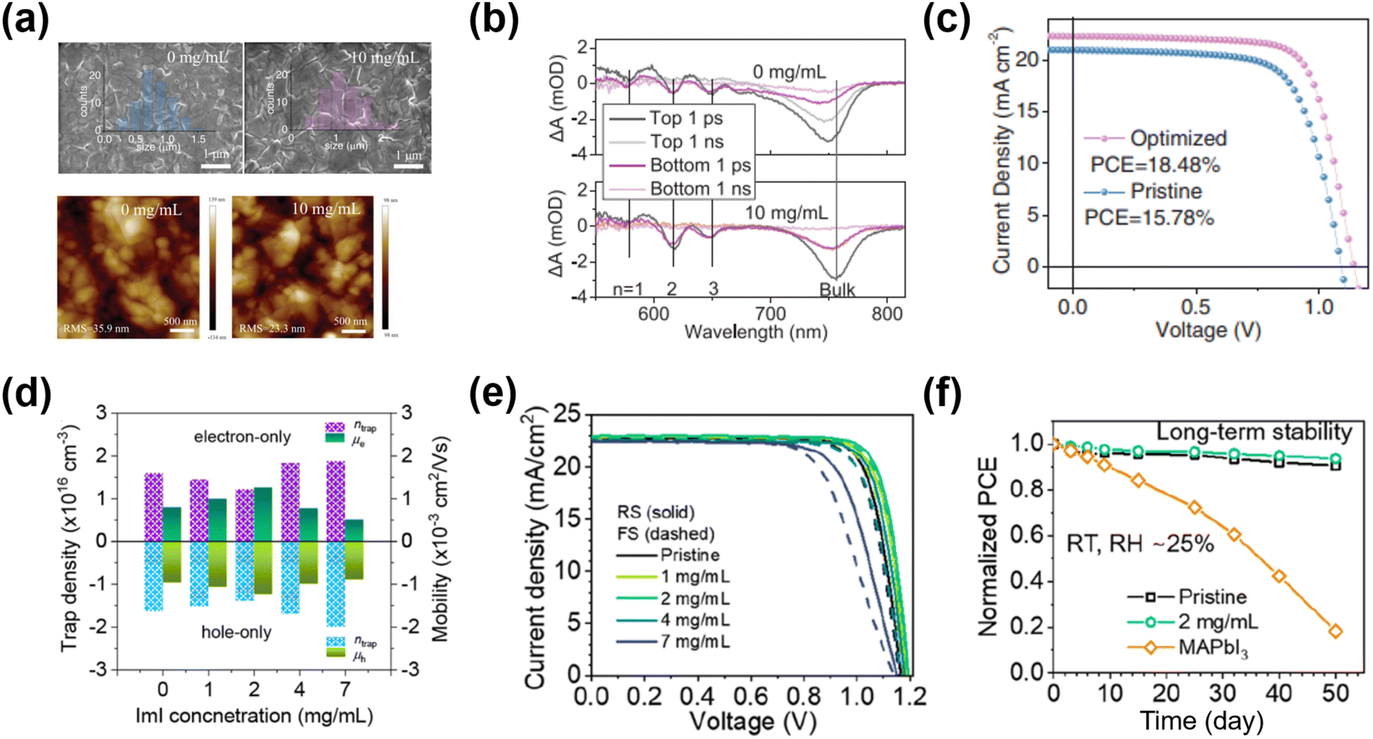
Zhang et al.65 optimized the crystallization process of the 2D ACI perovskite by solvent engineering–adopting a mixed solvent of dimethylformamide (DMF) and dimethyl sulfoxide (DMSO) at the volume ratio of 1:10. With the assistance of in situ grazing-incidence X-ray scattering (GIWAXS) characterization, it was found that 2D GA2PbI4 was the crucial intermediate phase, which provided the scaffold for the ACI perovskite growth, and dominated the distribution of GAMA3Pb3I10 (n = 3) with less of other n-value-phases and 1D GAPbI3 impurities. Additionally, the hot-casting method was used instead of traditional anti-solvent processing to effectively reduce the defect density. Consequently, the high-quality ACI perovskite film was deposited, yielding a greatly improved PCE of 14.7%.
Additive engineering also helps improve the crystallinity of the 2D GAMA3PbI10 (n = 3) perovskite films. Zhang et al.66 introduced MASCN (0.3 molar ratio relative to PbI2) in the perovskite precursor. Compared to the pristine 2D ACI perovskite film, the grain size in the MASCN-doped 2D ACI films was clearly enlarged, which was accompanied by high crystallinity. Eventually, the PCE of the device with the MASCN additive was boosted from 9.05% (non-doped) to 10.12%. Suitable additives also controlled the distribution of the targeted ACI quantum wells (QWs, i.e., the n number).67 Luo et al.64 effectively promoted the charge transfer of 2D ACI (n = 3) by adding MACl in the precursor solution. The optimized thickness distribution of the QWs decreased the carrier-populating time to 0.8 ps, which enabled highly efficient transport/extraction in PSCs (Fig. 7a and b). Meanwhile, the morphology of the 2D ACI became smoother with the increased grain size. After optimization, the MACl-treated device delivered a record PCE of 18.48% (Fig. 7c).
 | ||
| Fig. 7 The morphology of the 2D ACI film: (a) the top-view SEM images of the ACI films without/with MACl treatment (top); atomic force microscopy (AFM) images of the ACI films without/with MACl treatment. (b) Transient absorption (TA) spectra at different delay times for the ACI films without/with MACl treatment. (c) J–V curves under the reverse voltage scan of the best device ACI films without/with MACl treatment. Reproduced with permission.64 Copyright 2019, Wiley-VCH. (d) Trap density (ntrap) and mobility (μ) of the GA(MA)nPbnI3n+1 (n = 5) perovskite films with ImI treatment. (e) J–V curves under reverse- and forward-scan of PSCs with ImI treatment. (f) Long-term stability of PSCs without/with 2 mg mL−1 ImI treatment at RT and 25% RH for 50 days. Reproduced with permission.26 Copyright 2022, ACS Publishing Group. | ||
(GA)(MA)nPbnI3n+1 (n ≥ 4). As the n increases, the bandgap of 2D ACI approaches that of the 3D perovskites. Utilizing DMSO as a co-solvent to suppress lower n-phases could also be realized for n = 4 phase purification, according to the report by Ma et al.62 The DMSO in the precursor solution could obstruct the formation of the low-n (e.g., n = 1) phases in ACI perovskite films, resulting in reducing the hole-trap density and improving the charge transport. To give insight into the solvent influence on the crystallization of quasi-2D ACI, Yang et al.61 introduced a mixed solvent of DMSO/DMF (v
:v = 1:10) to increase the GAMA5Pb5I16 (n = 5) ACI formation. The stable intermediate phases can slow down the interposition of ions, which in turn retarded the crystallization of the ACI phases. Herein, the DMSO co-solvent led to a new intermediate solvate phase of MA2Pb3I8·2DMSO, whose solvation was immediately deprived along with the transition into ACI phases. The following thermal treatment completed the decomposition of intermediates and ACI crystallization with good film uniformity and surface coverage, leading to reduced charge recombination loss. Eventually, the unencapsulated PSCs realized a PCE of 19.8%.
Besides solvent engineering, post-treatment benefits the quasi-2D ACI phase arrangement. Zhang et al.63 proposed a sequential post-treatment method of modifying the GAMA4Pb4I13 ACI film with GASCN and MACl. GASCN could improve the quality of the perovskite films through the coordination bonding between SCN− and Pb2+, resulting in dense and well-aligned crystal grains. The sequential MACl treatment can suppress the charge defects on the perovskite surface and grain boundaries, which increased the electron/hole mobility. The PSCs based on sequential post-treatment demonstrated the best PCE of 15.27%, which was much higher than that of the pristine device (8.26%). Park et al.26 employed a post-treatment reagent of amphoteric imidazolium iodide (ImI) on the top of the ACI n = 5 perovskite film. ImI post-treatment effectively reduced the vacancies/excess defects of the perovskite (Fig. 7d). Consequently, lower trap density and higher charge mobility were achieved, yielding a record-high PCE of 22.26% among the ACI-based 2D PSCs (Fig. 7e and f).
No research studies have been focused on GA-based ACI PSCs with further increased n, perhaps because of their negligible structural and optical differences from the GA-doped 3D species. Despite additive and solvent engineering optimization, the parasitic 1D GAPbI3 or 2D GA2PbI4 within the 3D perovskite matrix during ACI crystallization could not be eliminated. Their insufficiency in light capture, the role of the carrier trap center, as well as the resulting nonuniformity in the film morphologies are the critical barrier to achieving highly efficient and stable ACI-based devices. More technologies are needed to obtain the highly pure 2D ACI phases.
4. Additive engineering
Additive engineering is widely utilized to improve photovoltaic performance and long-term stability performances. The effects of prohibiting uncoordinated defects and ion migration by N-contained lone-pair groups and the abundant hydrogen bonds from GA-based additives resemble that of GA-based dopants in A-site compositional engineering. Additionally, the ions could be inserted into the perovskite lattice and distort the perovskite structure in some cases, ameliorating structural and thermal stability.68,69 Other distinctive functions are presented in the promotion of uniform and compact perovskite films by modulating the crystallization process such as nucleation and growth, and bandgap alignment through self-doping effect.70,71 In most cases, the hydrophobic nature of the molecules also improves the ambient stability of the devices. GABr and GASCN are typically used as additives.72–74 The corresponding data are summarized in Table 5.| Additive | Perovskite component | Device configuration | PCE (%) | Stability | Ref. |
|---|---|---|---|---|---|
| GABr | FAxMAyCszPbI3−yBry | FTO/SnO2/PVSK/spiro-OMeTAD/Au | 20.29 | T 90 > 60 d in the air at 25 °C with 25% RH; T70 > 60 d in the air at 80 °C with 40% RH; T75 > 5 h in the air under 1 sun illumination | 72 |
| FAPbBr3 | ITO/SnO2/PVSK/spiro-OMeTAD/Au | 8.92 | T 90 > 1024 h in the air at RT with 50% RH | 75 | |
| FA0.7MA0.3Pb0.7Sn0.3I3 | ITO/EMICPEDOT:PSS/PVSK/S-acetylthiocholine chloride/C60/BCP/Ag | 20.63 | T 85 > 1000 h in the air at RT with 50–60% RH; T90 > 24 h in the air at 80 °C with 50–60% RH | 76 | |
| GA0.05Cs0.15FA0.8Pb(I0.85Br0.15)3 | FTO/SnO2/PVSK/spiro-MeOTAD/Au | 21.33 | T 80 > 8 h in N2 at MPP under 1 sun illumination | 77 | |
| GASCN | (FASnI3)0.6(MAPbI3)0.4 | ITO/PEDOT:PSS/PVSK/C60/BCP/Ag | 20.5 | T 80 = 220 h in N2 at MPP | 78 |
| (FASnI3)0.6(MAPbI3)0.4 | ITO/PEDOT:PSS/PVSK/C60/BCP/Ag | 22.1 Tandem: 25.4 | T 82 = 1830 h in N2 at 30–35 °C under 0.8 light soaking; T90 = 500 h in air | 79 | |
| PEA0.1FA0.9SnI3 | ITO/PEDOT:PSS/PVSK/PC61BM/poly-ethylenimine/Ag | 10.06 | T 91 = 720 h in N2 at 25 °C; T45 = 15 h in the air at 25 °C with 25% RH; T55 = 2 h in air at 25 °C with 60% RH | 80 | |
| FASnI3 | ITO/NiOx/PVSK/ICBA/BCP/Ag | 13.79 | T 90 = 1200 h in N2 | 81 | |
| GACl | CsMAFA/Pb/(I0.87Br0.13)3 | FTO/TiO2/PVSK/spiro-OMeTAD/Au | 17.9 | None | 82 |
| MAPbI3 | FTO/TiO2/ZrO2/PVSK/carbon layer | 14.35 | None | 73 | |
| GABF4 | MAPbI3 | ITO/NiOx/PVSK/PC61BM/Ag | 20.62 | T 81 = 45 d in the air at RT with 50–60% RH | 83 |
| GuaSO3NH2 | Cs0.05(MA0.12FA0.88)0.95Pb(I0.88Br0.12)3 | FTO/TiO2/PVSK/spiro-MeOTAD/Au | 21.66 | T 90 = 750 h in the air at RT with 25% RH | 84 |
| GAPbI2Br | CsPbI2Br | ITO/ZnO/PVSK/spiro-MeOTAD/Au | 14.34 | T 94 = 1000 h in N2 | 85 |
4.1 GABr additive
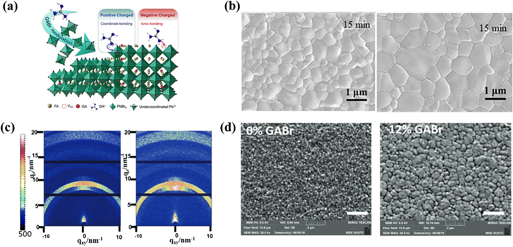
The multi-functional role of GABr was exemplified by Xu et al.75 Due to the ionized ammonium group (–NH3+) and unsaturated N atoms (–NH2 or![[double bond, length as m-dash]](https://www.rsc.org/images/entities/char_e001.gif) NH) in the GA+ cation, these two differently charged groups could be used to eliminate both positively charged (uncoordinated Pb2+) and negatively charged (I vacancy) defects to reduce nonradiative recombination (Fig. 8a). More noticeably, the grain size in the perovskite film with the GABr additive was increased from 600 nm to about 1 μm (Fig. 8b). The high-quality crystallization contributed to the reduced surface charge defects, and the mechanisms of morphology modulation were attributed to the incorporation of bulky GA+ into the perovskite lattice. Last, the band alignment between the perovskite and HTL became better. In contrast to the pristine device, the 15 wt.% GABr-doped devices showed a higher built-in potential (Vbi), which generated a strong driving force for intrinsic charge separation. These multiple factors together corresponded to the minimized VOC loss. The FAPbBr3-based wide band-gap device (Eg ∼ 2.3 eV) with GABr reached the PCE of 8.92% with a high VOC of 1.639 V.
NH) in the GA+ cation, these two differently charged groups could be used to eliminate both positively charged (uncoordinated Pb2+) and negatively charged (I vacancy) defects to reduce nonradiative recombination (Fig. 8a). More noticeably, the grain size in the perovskite film with the GABr additive was increased from 600 nm to about 1 μm (Fig. 8b). The high-quality crystallization contributed to the reduced surface charge defects, and the mechanisms of morphology modulation were attributed to the incorporation of bulky GA+ into the perovskite lattice. Last, the band alignment between the perovskite and HTL became better. In contrast to the pristine device, the 15 wt.% GABr-doped devices showed a higher built-in potential (Vbi), which generated a strong driving force for intrinsic charge separation. These multiple factors together corresponded to the minimized VOC loss. The FAPbBr3-based wide band-gap device (Eg ∼ 2.3 eV) with GABr reached the PCE of 8.92% with a high VOC of 1.639 V.
 | ||
| Fig. 8 (a) The schematic mechanism of GABr modulation on FAPbBr3-based PSCs. (b) Top-view SEM images of the control (left) and 15% GABr film (right) annealed at 110 °C for 15 min. Reproduced with permission.75 Copyright 2022, Elsevier. (c) 2D grazing-incidence X-ray diffraction (GIXRD) patterns of the perovskite films without (left) and with 12% GABr (right), respectively. (d) The SEM top images of the perovskite films without and with 12% GABr, respectively (the scale bar is 2 μm). Reproduced with permission.76 Copyright 2020, Elsevier. | ||
Despite the great promise of the Sn-Pb binary perovskite for developing low band-gap PSCs (Eg = 1.2–1.3 eV), it suffers from the enormous challenge of Sn2+ oxidation, leaving Sn vacancies. The defect elimination caused by Sn2+ oxidation could also be achieved by GABr addition, as reported by Zhou et al.76 In 2D GIXRD, the strongly dispersed secondary blots and bright rings in the perovskite film with 12% GABr additive demonstrated that the crystalline realms retained good orientation (Fig. 8d). Apart from the improved crystal quality and purity, GA+ was beneficial to the structural stability and restriction of the ion migration. Moreover, Br anions in the additive could act as a substituent on the X site to increase the tolerance factor and bandgap of the perovskites compared to those of the iodine-based ones.77,85 As a result, the device with 12% GABr obtained a PCE of 20.63% with negligible J–V hysteresis and superior environment and thermal stability.
4.2 GASCN additive
GASCN has been proven as another effective additive in PSCs, in which GA+ reduces defect states at the surface and boundary of the perovskite film due to the formation of hydrogen bonds. Meanwhile, SCN ions could regulate perovskite grain growth and again heal the defects in the grains of the perovskite film, owing to the Lewis-base nature of the S and N atoms in SCN.86,87 Furthermore, SCN− quickly is released from the perovskite films during the annealing process in the form of HSCN gas. Therefore, little residual GASCN remains.81,88 The oxidation of Sn2+ could also be suppressed by GASCN.78 In the charge-carrier dynamics, the (FASnI3)0.6(MAPbI3)0.4 perovskite film modified with 7% GASCN exhibited drastically prolonged PL lifetimes (∼1 μs), which was comparable to that of pure Pb–based perovskite thin films due to the noticeable low defect density (Fig. 9a). Furthermore, the device with GASCN modification achieved a PCE of over 20% in single-junction cells and 25% in the all-perovskite tandem device, respectively, which benefited from the increase in carrier lifetime (Fig. 9b and c). Similar results were also reported by some other groups to stabilize pure Sn-based perovskites.80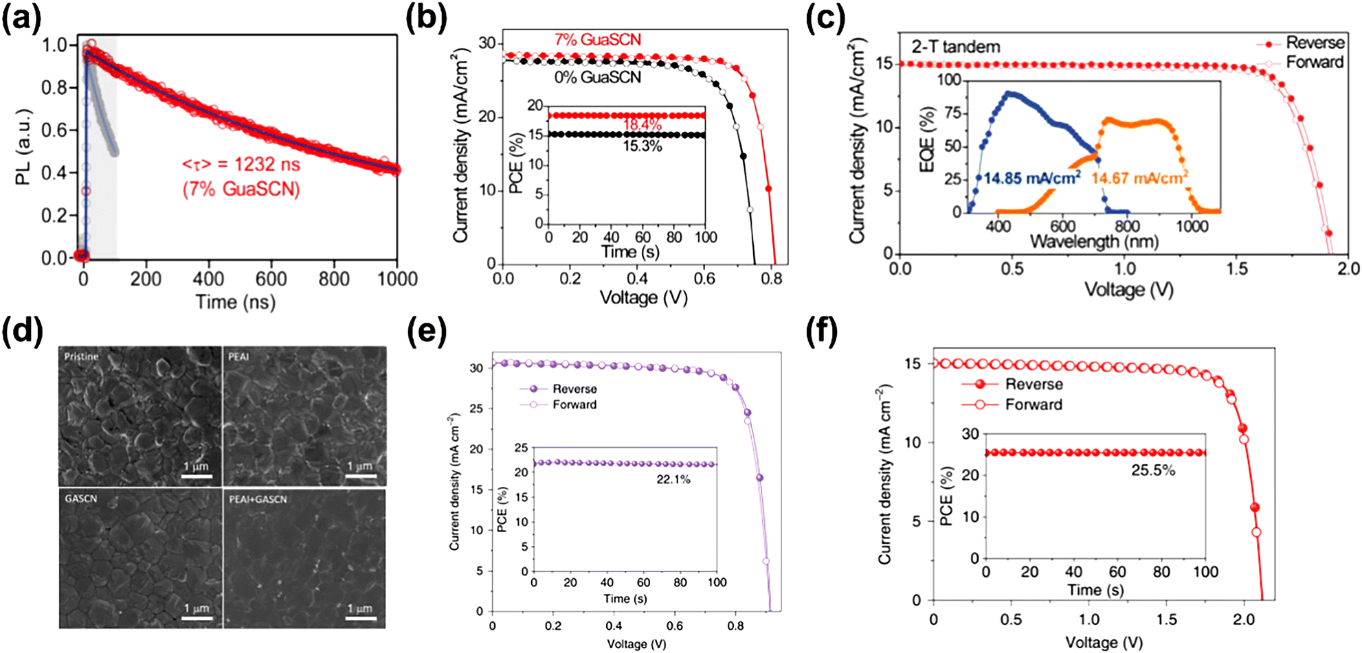 | ||
| Fig. 9 (a) Time-resolved photoluminescence of the perovskite film with GASCN. J–V curves of (b) the champion single PSC; the inset shows the SPO efficiency near the maximum power point (MPP), and (c) the 2-T tandem cell. The inset shows the EQE spectra of the top and bottom subcells, respectively. Reproduced with permission.78 Copyright 2019, AAAS. (d) Top-view SEM photograph of the perovskite film with PEAI and GASCN additives. J–V curves of (e) the single champion device with PEAI and GASCN additives along with the SPO efficiency, and (f) all-perovskite tandem PSCs along with the SPO. Reproduced with permission.79 Copyright 2022, Nature Publishing Group. | ||
Recently, PEASCN and GASCN additives have been employed in the Sn–Pb-based perovskite precursor.79 The binary cation additives helped form the quasi-2D (PEA)2GAPb2I7 deposited at the surfaces and grain boundaries to suppress more charge traps than that caused by Sn2+ oxidation (Fig. 9d). The 2D additive engineering endowed the Sn–Pb-based single-junction cells and two-terminal tandems with efficiencies of 22.1% and 25.5%, respectively (Fig. 9e and f).
4.3 Other GA-based additives
Anions such as Cl−, tetrafluoroborate (BF4−), and sulfamate (H2N–SO3−) in GA-based additives play a crucial and synergistic role, similar to SCN−. These anions could regulate the grain-size growth of perovskite films and passivate defects such as undercoordinated Pb2+ and Pb0, thus affecting the charge transfer behaviors and photovoltaic properties.Given that the O and N atoms of H2N–SO3(SM) could bond with uncoordinated Pb2+ because of the lone electron pairs in O and N, Liu et al.84 introduced GASM into the [Cs0.05(MA0.12FA0.88)0.95Pb(I0.88Br0.12)3] perovskite precursor to passivate charge traps at the surface and grain boundary effectively. With the dual-function synergy effect of GA+ and SM, the grain size of the perovskite film was enhanced, and the PL intensity of perovskite film became stronger. The optimal device yielded the best PCE of 21.66%, and kept 90% of its original efficiency after 800 h storage in ambient conditions.
Similar to GA-based dopants in A-site composition engineering, the content of GA-based additives is usually less than 20% (molar ratio vs. Pb species). A high concentration of GA-based additives would cause the formation of the impure phases, and the disruption of high-quality crystallization. Moreover, the anions could influence the GA incorporation in the perovskite lattice, which expands the lattice constant. A detailed mechanism of the synergistic effect of the GA+ cation and anion on the perovskite is still unclear, and requires further research.
5. Interface engineering
The interfaces of the ETL/perovskite and perovskite/HTL determine the efficiency of the charge transport, perovskite crystallization, and energy level adjustment.89,90 Such interface properties could be engineered by the GA-contained interface introduction, which functions as a conventional passivator or 2D perovskite passivation layer.91–93 Performances of PSCs with GA-based interface engineering are presented in Table 6.| Interface engineering layer | 3D perovskite layer | Device structure | PCE (%) | Stability | Ref. |
|---|---|---|---|---|---|
| PVSK: perovskite; RH: relative humidity; Tx is when PCE degrades to x% of the initial value. | |||||
| GACl | MAPbI3 | ITO/PTAA/PVSK/PC61BM/LiF/Al | 18.65 | None | 96 |
| GACl | MAPbI2.7Cl0.3 | FTO/TiO2/PVSK/spiroOMeTAD/Ag | 18.46 | T 95 > 22 d in N2 | 91 |
| GABr | CsPbI3 | FTO/TiO2/PVSK/PTAA/Au | 18.02 | T 92 > 30 d at 20–30% RH | 107 |
| GABr | FA0.8Cs0.2Pb(I0.7Br0.3)3 | ITO/PTAA/PVSK/C60/BCP/Ag | 18.19 | T 72 > 70 h at RT and > 50% RH in air | 74 |
| GABr | (FA0.95PbI2.95)0.85(MAPbBr3)0.15 | ITO/PTAA/PVSK/PC61BM/C60/BCP/Cu | 21.51 | T 95 = 500 h at 85 °C in N2 | 94 |
| GAI | MAPbI3 | ITO/SnO2/PVSK/spiroOMeTAD/Au | 18.54 | T 85 = 30 d in dry condition; T50 = 15 d in 60 ± 10% RH. | 52 |
| GAI | FAPbI3 | FTO/TiO2/PVSK/spiroOMeTAD/MgF2/Au | 24.36 | None | 95 |
| GASCN | MAPbI3 | FTO/TiO2/PVSK/spiroOMeTAD/Au | 21.26 | T 80 = 1000 h in the air at 20% RH | 97 |
| 1D GAPbI3 | (FA0.9Cs0.07MA0.03Pb(I0.92Br0.08)3 | FTO/TiO2/PVSK/spiroOMeTAD/Au | 21 | T 80 = 550 h in N2 at MPP under RT | |
| 2D GA2PbI4 | CsPbI2Br | FTO/SnO2/PVSK/spiroOMeTAD/Au | 15.6 | T 88 = 60 d in the air at 25 °C with 25% RH; T76 = 30 d in the air at 80 °C with 25% RH; T90 = 5 h in the air at MPP | 103 |
| 2D GA2PbI4 | n–i–p: Cs0.05FA0.85MA0.1PbI3 | n–i–p: ITO/SnO2/PVKS/spiroOMeTAD/Au | n–i–p: 20.1 | T 90 > 30 d in N2 | 99 |
| p–i–n: Cs0.3FA0.6DMA0.1PbI2.4Br0.6 | p–i–n: ITO/NiOx/PVKS/PC61BM/BCP/Ag | p–i–n: 22.9 | |||
| 2D GA2PbI4 | FA1−xMAxPbI3−xBrx | FTO/SnO2/PVKS/spiroOMeTAD/Au | 22.53 | T 90 > 30 d in the air with 25% RH; T80 > 30 d in the air with 75 ± 5% RH; T80 > 30 d in N2 under light illumination | 98 |
5.1 GA-cation passivation layer
GA-based salts are considered suitable alternatives for interface engineering because the GA cation could bond with the uncoordinated halogen by hydrogen bonds and uncoordinated Pb2+ or Pb clusters by lone pair electrons provided by N atoms, resulting in reduced trap sites.94,96 The added ion doping into the perovskite lattice was also observed in some cases, whose effects have attracted more comprehensive research. GA-based salts that have been reported as passivation agents so far are GA-halide salts (e.g., GAI, GABr, and GACl) and GASCN.Luo et al.94 spin-coated the multi-functional GABr on the surface of (FA0.95PbI2.95)0.85(MAPbBr3)0.15 perovskite film in the inverted PSCs. With the GABr passivation, the bright spots on the surface and boundaries disappeared, indicating that the PbX2 impurity was removed (Fig. 10a and b). Moreover, the GABr additive made the Fermi levels of the perovskite films shift toward the vacuum (400 mV), which was higher than the valence band upshift (200 mV), indicating more n-type nature after GABr treatment (Fig. 10c). The more n-type perovskite film could result in a larger fraction of occupied versus vacant traps, and a reduction in the rate of trap-assisted recombination. Additionally, Br enrichment was observed near the interface after the addition, leading to a wider bandgap (80 meV) in this region. It is energetically favorable for one or both charge carriers to reside predominantly within the bulk of the film, away from the surface defects. The device with GABr passivation delivered a PCE of 21.51% with a record VOC of 1.21 V, resulting from the suppression of trap-induced recombination (Fig. 10d).
 | ||
| Fig. 10 (a) Top view SEM images of the perovskite film with/without GABr passivation (upper panel). XRD patterns (lower panel) of the perovskite film with/without GABr treatment (α: black perovskite phase; β: non-perovskite phase). (b) Schematic energy-level diagrams of the control and GABr-treated films. (c) J–V curves under the reverse scan of devices with/without GABr passivation. Reproduced with permission.94 Copyright 2018, AAAS. (d) Top view SEM images of the perovskite film with/without binary GAI/tBPMAI treatment. (e) The time-of-flight secondary-ion mass spectrometry (ToF-SIMS) of the binary GAI/tBPMAI-treated perovskite film. (f) The forward/reverse scan J–V curves of the best devices with/without the binary GAI/tBPMAI treatment. Reproduced with permission.95 Copyright 2021, Royal Society of Chemistry. | ||
Sometimes, GA-based passivation agents were simultaneously post-treated along with other salts for more progress. Zhang et al.95 addressed the complete passivation from the interfaces to bulk in the perovskite film by combining GAI with 4-tert-butyl-phenylmethylammonium iodide (tBPMAI) as the passivation agent. Given the difference between GAI and tBPMAI in ionic radius, GA could diffuse into the perovskite lattice. At the same time, the tBPMAI gathered on the surface of the perovskite, simultaneously modulating defects in perovskites from bulk to interfaces, which were confirmed by ToF-SIMS (Fig. 10f). More interestingly, it showed a positive effect on crystallization modulation after the post-treatment of this composite layer. The perovskite grains were regularly arranged, leading to the compact and smooth morphology of the perovskite (Fig. 10e). Finally, the device with individual GAI or tBPMAI treatment showed a low PCE of 21.79%. In contrast, the device with binary passivation obtained the champion PCE of 24.36% with a lower voltage loss of 0.388 V (Fig. 10g).
Better crystal growth with fewer trap states also can be regulated by the passivator itself and its solvent. Yang et al.97 selected GASCN dissolved in chlorobenzene (CB) anti-solvent to passivate the MAPbI3 surface effectively. The GA cation could stabilize the black phase, anchor the lattice ion, and inhibit their migration due to the hydrogen bond formation. Results from different anti-solvents such as ethyl acetate (EA), i-propanol (IPA), and cyclohexane (CH) were also discussed here. Compared with other anti-solvents, CB with low polarity could cause minor damage to the perovskite grain and slow down the crystallization process. As a synergistic result of GASCN and CB, the grain size was dramatically increased. This binary strategy increased the PCE from 20.14% to 21.26%, and the thermal and moisture stability were enhanced.
The functions of constructing a GA-based interface (defect passivation, energy level alignment, and crystallization regulation) are similar to that of GA-based additives. However, this approach induces two individual layers, different from the doping behavior of additives in the perovskite layer during additive engineering. So, the limits of the GA molar ratio (vs. overall A-site cation content) considering the possible interference on perovskite crystallization are not involved here. However, the limits lie in its low solubility in CB. Generally, IPA is chosen to dissolve the GA-based agents, but as mentioned before, IPA could erode the surface of the perovskite film owing to the relatively high polarity. Searching for a low-polarized anti-solvent that is compatible with GA salts or exploring soluble GA salts in CB should be the future task for managing GA-contained interfaces.
5.2 2D perovskite passivation layer
Recently, the PCE of PSCs with 2D/3D structure has surprisingly achieved 25%, comparable to that of crystalline silicon-based commercial PV products. The 2D perovskite passivation layer has been produced for various functions, from passivating surface defects of 3D perovskite and energy level alignment to improving resistance to environmental stress.100–102 Given the high hydrophobicity of 2D GAn+1PbnI3n+1, devices comprising the 2D/3D form exhibit significantly improved environmental stability compared to devices containing only the 3D perovskite.103,104 2D passivation layers could be prepared by solution processing, immersion processing, vacuum deposition, and mechanical press as standard,105 but unconventionally, it was a new phase induced by the interaction between dopants and the surface perovskite layers.Similar to the dual optimization scheme introduced previously,95 Zhang et al.98 treated the perovskite with GAI and GACl to realize surface and bulk modification. Theoretical calculations proposed that among GAX salts, the Cl doping system exhibited the highest formation energy of iodine vacancy and the longest excited state lifetime. Therefore, GACl was expected to be an appropriate passivator for bulk doping, and the outperformed PCE of GACl (20.07%) was higher than others (17.71% for GABr and 18.01% for GAI). However, the smallest ionic radius of Cl−, showing the lowest activation energy barrier for X ion migration, infers the need to suppress its bulk diffusion to the surface. Co-doping with GAI was suggested to form a stable capping layer owing to its larger activation energy barrier (Fig. 11a and b). After co-doping, GAI was inserted into the 3D perovskite lattice forming the 2D GA2PbI4 layer for surface passivation (Fig. 11c). The incorporation of large GA cations also modulated the lattice tensile strain towards minimizing defect centers. Benefiting from the strategy for reducing nonradiative recombination centers from both bulk and interfacial regions and the energy level alignment after 2D layer insertion, the PCE of the device with a 2D/3D perovskite structure exceeded 22.53%. Moreover, the PCE maintained more than 90% after 30 days at 40% R.H. due to the enhanced hydrophobicity of the 2D layers.
 | ||
| Fig. 11 (a) Illumination of the halogen ion interstitial (Cli−/Bri−/Ii−) migration from the perovskite bulk (defined as initial state, IS) to the surface (defined as the final state, FS), along with (d) the energy profile. (b) The activation energy barrier of the halogen ion. (c) J–V curves under the reverse scan of devices with/without 2D perovskite passivation. Reproduced with permission.98 Copyright 2022, Wiley-VCH. (d) The average binding energy of different cations with NiOx surface by DFT. (e) Structural model and corresponding schematics of the crystallization process for films with varying concentrations of GA on NiOx. (f) The forward/reverse scan J–V curves of the champion devices with/without 2D perovskite passivation. Reproduced with permission.99 Copyright 2021, Wiley-VCH. | ||
The 2D perovskite layer not only passivates the 3D perovskite layer, but also shows the great potential of passivating buried side. Chen et al.99 introduced the 2D GA2PbI4 passivation layer in the inverted PSCs between NiOx HTL and the perovskite layer. The GA in 2D GA2PbI4 could connect with NiOx by forming hydrogen bonds, suppressing the migration of oxygen vacancies on the NiOx surface. In addition, the symmetric structure of GA promoted its accumulation onto the NiOx surface to suppress non-radiative recombination (Fig. 11e). It was special when other cations such as n-butylammonium (BA), ethylammonium (EA), and dimethylammonium (DMA) were also added to the precursor. It was found that DMA and EA could not form the 2D perovskite. Furthermore, the 2D BA-based perovskite phase was not present in the NiOx/perovskite interface, but was located in bulk. The authors ascribed the unique phenomenon to the GA cation's higher binding energy and polarity action (Fig. 11d). Finally, the inverted device boosted the PCE up to 22.9% with an increase of 65 mV in VOC (Fig. 11f).
It should not be ignored that in some cases, other low-dimensional phases would form when a GA-contained solution is spin-coated on top of a pre-formed 3D perovskite layer, which also shows a good passivation effect and interfacial band alignment. For instance, Alharbi et al.106 utilized solid-state magic angle spinning (MAS) NMR to verify the coexistence of 1D GAPbI3 and 2D GA2PbI4 on the surface of FA0.93Cs0.07PbI3. Similarly, Chavan et al.104 spin-coated GAI/IPA on the surface of a 3D perovskite film and detected the 1D δ-FAPbI3-like phase. Empirically, the formation of the GA-based 2D perovskite passivation interface is probably accompanied by the complicated mixture of the original GA-based precursors, 3D perovskite constitutes, or other 2D species with different QWs. However, it does not mean that there are positive contributions from every impurity, or in many cases. Moreover, the inefficiency in charge transport across the organic interlayer and the light conversion due to the wider bandgap becomes intrinsic drawbacks of 2D materials. Delicate control for pristine or specific composites in 2D interlayers, as well as the design of innovative 2D materials with better intrinsic properties, should be valued in the future.
6. Summary and perspective
In summary, in light of the processing approaches for introducing the guanidinium cation, we systematically reviewed recent research and development on the application of GA in PSCs, including A-site substitution in either 3D perovskite or 2D ACI perovskite, additive, and interface engineering. The series of breakthroughs showed that GA cations exhibited unique potential in addressing the coexistence of long-term operational stability issues and effective photovoltaic performance in PSCs. Despite these merits, efforts toward some intractable challenges remain to be emphasized as follows:(1) Choosing the proper anion in GA salts for improving the performance of PSCs. Nowadays, GA-based salts have been widely used in the field of PSCs, and the anion is another factor for defect passivation, energy alignment, and structure stabilization. For example, Cl− could tune the crystallization process, and Br− could change the charge distribution and bandgap of the perovskite surface. SCN− and BF4− could effectively passivate defects such as undercoordinated Pb ions in the bulk and interface due to lone pair electrons. As a result, a suitable anion is a key aspect to eliminate charge defects.
(2) Developing a more moisture-resistant GA-based perovskite. Due to the lack of long hydrophobic chains or ring structures, the GA-based perovskite film degrades faster than DJ or RP perovskites under moisture and thermal stresses. Therefore, it should be taken into consideration to introduce the new GA-based derivatives for long-term operation stability, but the relevant papers are limited.108,109 In addition, it is an alternative way to take the place of GA by long-chain cations as the interlayer cations phase to endow more hydrophobic properties, thereby increasing moisture repellence and stability for ACI perovskites.110 Few reports are applying monovalent cations (e.g., Cs and FA) to replace MA. Regarding the effect of steric hindrance on the perovskite structure, the cations with appropriate ionic radius are expected to be better candidates to alternate with GA than MA.
(3) Constructing the new 2D GA-based ACI capping layer on top of the 3D perovskite. Although GA2PbI4 was shown to passivate the surface defects of the 3D perovskite and prevent moisture from damaging the perovskite structure, its poor charge mobility inhibits efficient device operation. The 2D ACI layer with large n is expected to be a competitive alternative as the capping layer due to the high carrier mobility. It is noted that when the 2D ACI perovskite is deposited on the surface of 3D perovskite, the formation of multiple-perovskite phases would be induced, including (GA)x(MA)1−xPbI3, GA2PbI4, or other GA-based ACI with different quantum wells (n), which are possible trap sites on the surface. More precise control towards n should be valued in the future.
(4) Further investigating the photophysical behavior in GA-based perovskites, especially ACI systems. The mechanisms of charge carrier dynamics, phase degradation, and ion migration in 2D ACI have not been systematically studied. A comprehensive understanding of these evolutions would provide critical guides for improving photovoltaic performances. Moreover, it would help ACI materials to become competitive candidates for application in other semiconducting fields, including photodetectors, light-emitting diodes, or field-effect transistors.
(5) Application in other photoelectric devices. In addition to PSCs, the GA-based perovskite materials demonstrated excellent performance in the area of the optoelectrical device including light-emitting diodes (LEDs) and photodetectors.111,112 Similar to solar cells, the GA could treat the surface of nanocrystals or colloidal quantum dots113,114 to passivate the defects and provides lattice-stabilizing effect via hydrogen bonds, reducing non-radiative recombination. Further research studies are still needed to define the “insight” mechanism.
Conflicts of interest
The authors declare no conflict of interest.Acknowledgements
This work was financially supported by the National Key Research and Development Program of China (2021YFB3800103), the Fundamental Research Funds for the Central Universities (000-0903069032), and the National Natural Science Foundation of China (52203237).References
- F. Zhang, S. Y. Park, C. Yao, H. Lu, S. P. Dunfield, C. Xiao, S. Uličná, X. Zhao, L. D. Hill, X. Chen, X. Wang, L. E. Mundt, K. H. Stone, L. T. Schelhas, G. Teeter, S. Parkin, E. L. Ratcliff, Y.-L. Loo, J. J. Berry, M. C. Beard, Y. Yan, B. W. Larson and K. Zhu, Metastable Dion-Jacobson 2D structure enables efficient and stable perovskite solar cells, Science, 2022, 375, 71–76 CrossRef CAS PubMed.
- X. Zhao, T. Liu, Q. C. Burlingame, T. Liu, R. Holley III, G. Cheng, N. Yao, F. Gao and Y.-L. Loo, Accelerated aging of all-inorganic, interface-stabilized perovskite solar cells, Science, 2022, 377, 307–310 CrossRef CAS PubMed.
- M. Kim, J. Jeong, H. Lu, T. K. Lee, F. T. Eickemeyer, Y. Liu, I. W. Choi, S. J. Choi, Y. Jo, H.-B. Kim, S.-I. Mo, Y.-K. Kim, H. Lee, N. G. An, S. Cho, W. R. Tress, S. M. Zakeeruddin, A. Hagfeldt, J. Y. Kim, M. Grätzel and D. S. Kim, Conformal quantum dot–SnO2 layers as electron transporters for efficient perovskite solar cells, Science, 2022, 375, 302–306 CrossRef CAS PubMed.
- J. Jeong, M. Kim, J. Seo, H. Lu, P. Ahlawat, A. Mishra, Y. Yang, M. A. Hope, F. T. Eickemeyer, M. Kim, Y. J. Yoon, I. W. Choi, B. P. Darwich, S. J. Choi, Y. Jo, J. H. Lee, B. Walker, S. M. Zakeeruddin, L. Emsley, U. Rothlisberger, A. Hagfeldt, D. S. Kim, M. Grätzel and J. Y. Kim, Pseudo-halide anion engineering for α-FAPbI3 perovskite solar cells, Nature, 2021, 592, 381–385 CrossRef CAS PubMed.
- H. Min, D. Y. Lee, J. Kim, G. Kim, K. S. Lee, J. Kim, M. J. Paik, Y. K. Kim, K. S. Kim, M. G. Kim, T. J. Shin and S. Il Seok, Perovskite solar cells with atomically coherent interlayers on SnO2 electrodes, Nature, 2021, 598, 444–450 CrossRef CAS PubMed.
- P. Wu, S. Wang, X. Li and F. Zhang, Advances in SnO2-based perovskite solar cells: from preparation to photovoltaic applications, J. Mater. Chem. A, 2021, 9, 19554–19588 RSC.
- H. Zhu, Y. Ren, L. Pan, O. Ouellette, F. T. Eickemeyer, Y. Wu, X. Li, S. Wang, H. Liu, X. Dong, S. M. Zakeeruddin, Y. Liu, A. Hagfeldt and M. Grätzel, Synergistic effect of fluorinated passivator and hole transport dopant enables stable perovskite solar cells with an efficiency near 24%, J. Am. Chem. Soc., 2021, 143, 3231–3237 CrossRef CAS PubMed.
- R. Azmi, E. Ugur, A. Seitkhan, F. Aljamaan, A. S. Subbiah, J. Liu, G. T. Harrison, M. I. Nugraha, M. K. Eswaran, M. Babics, Y. Chen, F. Xu, T. G. Allen, A. u. Rehman, C.-L. Wang, T. D. Anthopoulos, U. Schwingenschlögl, M. De Bastiani, E. Aydin and S. De Wolf, Damp heat–stable perovskite solar cells with tailored-dimensionality 2D/3D heterojunctions, Science, 2022, 376, 73–77 CrossRef CAS PubMed.
- G. Yang, Z. Ren, K. Liu, M. Qin, W. Deng, H. Zhang, H. Wang, J. Liang, F. Ye, Q. Liang, H. Yin, Y. Chen, Y. Zhuang, S. Li, B. Gao, J. Wang, T. Shi, X. Wang, X. Lu, H. Wu, J. Hou, D. Lei, S. K. So, Y. Yang, G. Fang and G. Li, Stable and low-photovoltage-loss perovskite solar cells by multifunctional passivation, Nat. Photonics, 2021, 15, 681–689 CrossRef CAS.
- H. Kim, S. U. Lee, D. Y. Lee, M. J. Paik, H. Na, J. Lee and S. I. Seok, Optimal interfacial engineering with different length of alkylammonium halide for efficient and stable perovskite solar cells, Adv. Energy Mater., 2019, 9, 1902740 CrossRef CAS.
- T. Kodalle, R. F. Moral, L. Scalon, R. Szostak, M. Abdelsamie, P. E. Marchezi, A. F. Nogueira and C. M. Sutter-Fella, Revealing the transient formation dynamics and optoelectronic properties of 2D ruddlesden-popper phases on 3D perovskites, Adv. Energy Mater., 2022, 2201490 CrossRef.
- Y. Chen and H. Zhou, Defects chemistry in high-efficiency and stable perovskite solar cells, J. Appl. Phys., 2020, 128, 060903 CrossRef CAS.
- W. Li, S. Sidhik, B. Traore, R. Asadpour, J. Hou, H. Zhang, A. Fehr, J. Essman, Y. Wang, J. M. Hoffman, I. Spanopoulos, J. J. Crochet, E. Tsai, J. Strzalka, C. Katan, M. A. Alam, M. G. Kanatzidis, J. Even, J.-C. Blancon and A. D. Mohite, Light-activated interlayer contraction in two-dimensional perovskites for high-efficiency solar cells, Nat. Nanotechnol., 2022, 17, 45–52 CrossRef CAS PubMed.
- J. Y. Kim, J.-W. Lee, H. S. Jung, H. Shin and N.-G. Park, High-efficiency perovskite solar cells, Chem. Rev., 2020, 120, 7867–7918 CrossRef CAS PubMed.
- X. Wang, L. Cai, Y. Zou, D. Liang, L. Wang, Y. Li, J. Zang, G. Bai, X. Gao, T. Song and B. Sun, Unveiling the critical role of ammonium bromide in blue emissive perovskite films, Nanoscale, 2021, 13, 13497–13505 RSC.
- Y.-H. Kim, S. Kim, A. Kakekhani, J. Park, J. Park, Y.-H. Lee, H. Xu, S. Nagane, R. B. Wexler, D.-H. Kim, S. H. Jo, L. Martínez-Sarti, P. Tan, A. Sadhanala, G.-S. Park, Y.-W. Kim, B. Hu, H. J. Bolink, S. Yoo, R. H. Friend, A. M. Rappe and T.-W. Lee, Comprehensive defect suppression in perovskite nanocrystals for high-efficiency light-emitting diodes, Nat. Photonics, 2021, 15, 148–155 CrossRef CAS.
- G. Giorgi, J.-I. Fujisawa, H. Segawa and K. Yamashita, Organic–inorganic hybrid lead iodide perovskite featuring zero dipole moment guanidinium cations: a theoretical analysis, J. Phys. Chem. C, 2015, 119, 4694–4701 CrossRef CAS.
- W. Li, Z. Wang, F. Deschler, S. Gao, R. H. Friend and A. K. Cheetham, Chemically diverse and multifunctional hybrid organic–inorganic perovskites, Nat. Rev. Mater., 2017, 2, 1–18 Search PubMed.
- Y. Zhou, H. Xue, Y.-H. Jia, G. Brocks, S. Tao and N. Zhao, Enhanced incorporation of guanidinium in formamidinium-based perovskites for efficient and stable photovoltaics: the role of Cs and Br, Adv. Funct. Mater., 2019, 29, 1905739 CrossRef CAS.
- F. Zhang, B. Cai, J. Song, B. Han, B. Zhang and H. Zeng, Efficient blue perovskite light-emitting diodes boosted by 2D/3D energy cascade channels, Adv. Funct. Mater., 2020, 30, 2001732 CrossRef CAS.
- S. R. Pering, W. Deng, J. R. Troughton, P. Kubiak, D. Ghosh, R. Niemann, F. Brivio, F. Jeffrey, A. Walker, M. Islam, T. M. Watson, P. R. Raithby, A. L. Johnson, S. E. Lewis and P. J. Cameron, Azetidinium lead iodide for perovskite solar cells, J. Mater. Chem. A, 2017, 5, 20658–20665 RSC.
- S. Maheshwari, S. Patwardhan, G. C. Schatz, N. Renaud and F. C. Grozema, The effect of the magnitude and direction of the dipoles of organic cations on the electronic structure of hybrid halide perovskites, Phys. Chem. Chem. Phys., 2019, 21, 16564–16572 RSC.
- Computational Chemistry Comparison and Benchmark DataBase Release 22 (May 2022) Standard Reference Database, https://cccbdb.nist.gov/introx.asp.
- X. A. Jeanbourquin, X. Li, C. Law, P. R. Barnes, R. Humphry-Baker, P. Lund, M. I. Asghar and B. C. O’Regan, Rediscovering a key interface in dye-sensitized solar cells: guanidinium and iodine competition for binding sites at the dye/electrolyte surface, J. Am. Chem. Soc., 2014, 136, 7286–7294 CrossRef CAS PubMed.
- N. De Marco, H. Zhou, Q. Chen, P. Sun, Z. Liu, L. Meng, E.-P. Yao, Y. Liu, A. Schiffer and Y. Yang, Guanidinium: a route to enhanced carrier lifetime and open-circuit voltage in hybrid perovskite solar cells, Nano Lett., 2016, 16, 1009–1016 CrossRef PubMed.
- Y. Zhang and N.-G. Park, Quasi-Two-Dimensional Perovskite Solar Cells with Efficiency Exceeding 22%, ACS Energy Lett., 2022, 7, 757–765 CrossRef CAS.
- F. Zhang, H. Lu, J. Tong, J. J. Berry, M. C. Beard and K. Zhu, Advances in two-dimensional organic–inorganic hybrid perovskites, Energy Environ. Sci., 2020, 13, 1154–1186 RSC.
- X. Xu, X. Zhang, W. Deng, J. Jie and X. Zhang, 1D organic–inorganic hybrid perovskite micro/nanocrystals: fabrication, assembly, and optoelectronic applications, Small Methods, 2018, 2, 1700340 CrossRef.
- S. Sun, M. Lu, X. Gao, Z. Shi, X. Bai, W. W. Yu and Y. Zhang, 0D perovskites: unique properties, synthesis, and their applications, Adv. Sci., 2021, 8, 2102689 CrossRef PubMed.
- J. Ma, H. Wang and D. Li, Recent progress of chiral perovskites: materials, synthesis, and properties, Adv. Mater., 2021, 33, 2008785 CrossRef CAS PubMed.
- S. Ramos-Terrón, A. D. Jodlowski, C. Verdugo-Escamilla, L. Camacho and G. de Miguel, Relaxing the goldschmidt tolerance factor: sizable incorporation of the guanidinium cation into a two-dimensional ruddlesden–popper perovskite, Chem. Mater., 2020, 32, 4024–4037 CrossRef.
- H. Li, D. Wines, B. Chen, K. Yumigeta, Y. M. Sayyad, J. Kopaszek, S. Yang, C. Ataca, E. H. Sargent and S. Tongay, Abnormal phase transition and band renormalization of guanidinium-based organic–inorganic hybrid perovskite, ACS Appl. Mater. Interfaces, 2021, 13, 44964–44971 CrossRef CAS PubMed.
- S. Kanno, Y. Imamura and M. Hada, First-Principles calculations of the rotational motion and hydrogen bond capability of large organic cations in hybrid perovskites, J. Phys. Chem. C, 2018, 122, 15966–15972 CrossRef CAS.
- O. Nazarenko, M. R. Kotyrba, S. Yakunin, M. Aebli, G. Rainò, B. M. Benin, M. Wörle and M. V. Kovalenko, Guanidinium-formamidinium lead iodide: a layered perovskite-related compound with red luminescence at room temperature, J. Am. Chem. Soc., 2018, 140, 3850–3853 CrossRef CAS PubMed.
- E. Vega, M. Mollar and B. Marí, Effect of guanidinium on the optical properties and structure of the methylammonium lead halide perovskite, J. Alloys Compd., 2018, 739, 1059–1064 CrossRef CAS.
- A. D. Jodlowski, A. Yépez, R. Luque, L. Camacho and G. de Miguel, Benign-by-design solventless mechanochemical synthesis of three-, two-, and one-dimensional hybrid perovskites, Angew. Chem., Int. Ed., 2016, 55, 14972–14977 CrossRef CAS PubMed.
- M. Szafrański, Investigation of phase instabilities in guanidinium halogenoplumbates(II), Thermochim. Acta, 1997, 307, 177–183 CrossRef.
- S. Wang, S. Pang, D. Chen, W. Zhu, H. Xi and C. Zhang, Improving perovskite solar cell performance by compositional engineering via triple-mixed cations, Sol. Energy, 2021, 220, 412–417 CrossRef CAS.
- X. Li, K. Li, B. Wang, X. Zhang, S. Yue, Y. Li, Q. Chen, S. Li, T. Yue, H. Zhou and Y. Zhang, Efficient and stable Quasi-2D perovskite solar cells enabled by thermal-aged precursor solution, Adv. Funct. Mater., 2021, 31, 2107675 CrossRef CAS.
- C. Yi, J. Luo, S. Meloni, A. Boziki, N. Ashari-Astani, C. Grätzel, S. M. Zakeeruddin, U. Röthlisberger and M. Grätzel, Entropic stabilization of mixed A-cation ABX 3 metal halide perovskites for high performance perovskite solar cells, Energy Environ. Sci., 2016, 9, 656–662 RSC.
- M. Saliba, T. Matsui, K. Domanski, J.-Y. Seo, A. Ummadisingu, S. M. Zakeeruddin, J.-P. Correa-Baena, W. R. Tress, A. Abate, A. Hagfeldt and M. Grätzel, Incorporation of rubidium cations into perovskite solar cells improves photovoltaic performance, Science, 2016, 354, 206–209 CrossRef CAS PubMed.
- M. Saliba, T. Matsui, J.-Y. Seo, K. Domanski, J.-P. Correa-Baena, M. K. Nazeeruddin, S. M. Zakeeruddin, W. Tress, A. Abate, A. Hagfeldt and M. Grätzel, Cesium-containing triple cation perovskite solar cells: improved stability, reproducibility and high efficiency, Energy Environ. Sci., 2016, 9, 1989–1997 RSC.
- A. D. Jodlowski, C. Roldán-Carmona, G. Grancini, M. Salado, M. Ralaiarisoa, S. Ahmad, N. Koch, L. Camacho, G. De Miguel and M. K. Nazeeruddin, Large guanidinium cation mixed with methylammonium in lead iodide perovskites for 19% efficient solar cells, Nat. Energy, 2017, 2, 972–979 CrossRef CAS.
- K. Wang, S. Ma, X. Xue, T. Li, S. Sha, X. Ren, J. Zhang, H. Lu, J. Ma, S. Guo, Y. Liu, J. Feng, A. Najar and S. Liu, Highly efficient and stable CsPbTh3 (Th= I, Br, Cl) perovskite solar cells by combinational passivation strategy, Adv. Sci., 2022, 9, 2105103 CrossRef CAS PubMed.
- P.-K. Kung, K.-I. Lin, C.-S. Wu, M.-H. Li, C.-R. Chan, R. Rajendran, C.-F. Lin and P. Chen, Visualization of ion migration in an inorganic mixed halide perovskite by one-photon and multiphoton absorption: effect of guanidinium A-site cation incorporation, J. Phys. Chem. Lett., 2022, 13, 6944–6955 CrossRef CAS PubMed.
- L. Gao, X. Li, Y. Liu, J. Fang, S. Huang, I. Spanopoulos, X. Li, Y. Wang, L. Chen, G. Yang and M. G. Kanatzidis, Incorporated guanidinium expands the CH3NH3PbI3 lattice and enhances photovoltaic performance, ACS Appl. Mater. Interfaces, 2020, 12, 43885–43891 CrossRef CAS PubMed.
- D. J. Kubicki, D. Prochowicz, A. Hofstetter, M. Saski, P. Yadav, D. Bi, N. Pellet, J. Lewinski, S. M. Zakeeruddin, M. Grätzel and L. Emsley, Formation of stable mixed guanidinium–methylammonium phases with exceptionally long carrier lifetimes for high-efficiency lead iodide-based perovskite photovoltaics, J. Am. Chem. Soc., 2018, 140, 3345–3351 CrossRef CAS PubMed.
- G. S. Kumar, P. K. Sarkar, B. Pradhan, M. Hossain, K. Rao and S. Acharya, Large-area transparent flexible guanidinium incorporated MAPbI3 microstructures for high-performance photodetectors with enhanced stability, Nanoscale Horiz., 2020, 5, 696–704 RSC.
- F. B. Minussi, E. M. Bertoletti, S.P. Reis, J. F. Carvalho and E. B. Araújo, Guanidinium substitution-dependent phase transitions, ionic conductivity, and dielectric properties of MAPbI3, Chem. Commun., 2022, 58, 2212–2215 RSC.
- D. W. Ferdani, S. R. Pering, D. Ghosh, P. Kubiak, A. B. Walker, S. E. Lewis, A. L. Johnson, P. J. Baker, M. S. Islam and P. J. Cameron, Partial cation substitution reduces iodide ion transport in lead iodide perovskite solar cells, Energy Environ. Sci., 2019, 12, 2264–2272 RSC.
- R. J. Stoddard, A. Rajagopal, R. L. Palmer, I. L. Braly, A. K.-Y. Jen and H. W. Hillhouse, Enhancing defect tolerance and phase stability of high-bandgap perovskites via guanidinium alloying, ACS Energy Lett., 2018, 3, 1261–1268 CrossRef CAS.
- S. Wang, Y. Zhu, W. Sun, X. Miao, Z. Ma, C. Yang, B. Liu, S. Li, R. Ma and C. Wang, Large guanidinium cation enhance photovoltage for perovskite solar cells via solution-processed secondary growth technique, Sol. Energy, 2018, 176, 118–125 CrossRef CAS.
- N. D. Pham, C. Zhang, V. T. Tiong, S. Zhang, G. Will, A. Bou, J. Bisquert, P. E. Shaw, A. Du, G. J. Wilson and H. Wang, Tailoring crystal structure of FA0.83Cs0.17PbI3 perovskite through guanidinium doping for enhanced performance and tunable hysteresis of planar perovskite solar cells, Adv. Funct. Mater., 2019, 29, 1806479 CrossRef.
- Z. Li, L. Hao, D. Liu, X. Sun, Q. Zhao, Z. Shao, C. Chen, X. Wang, L. Wang, G. Cui and S. Pang, Inhibiting ion migration by guanidinium cation doping for efficient perovskite solar cells with enhanced operational stability, Sol. RRL, 2022, 6, 2200003 CrossRef CAS.
- I. Susic, L. Gil-Escrig, F. Palazon, M. Sessolo and H. J. Bolink, Quadruple-cation wide-bandgap perovskite solar cells with enhanced thermal stability enabled by vacuum deposition, ACS Energy Lett., 2022, 7, 1355–1363 CrossRef CAS PubMed.
- C. M. M. Soe, C. C. Stoumpos, M. Kepenekian, B. Traoré, H. Tsai, W. Nie, B. Wang, C. Katan, R. Seshadri, A. D. Mohite, J. Even, T. J. Marks and M. G. Kanatzidis, New type of 2D perovskites with alternating cations in the interlayer space,(C(NH2)3)(CH3NH3)nPbnI3n+1: Structure, properties, and photovoltaic performance, J. Am. Chem. Soc., 2017, 139, 16297–16309 CrossRef CAS PubMed.
- O. Nazarenko, M. R. Kotyrba, M. Wörle, E. Cuervo-Reyes, S. Yakunin and M. V. Kovalenko, Luminescent and photoconductive layered lead halide perovskite compounds comprising mixtures of cesium and guanidinium cations, Inorg. Chem., 2017, 56, 11552–11564 CrossRef CAS PubMed.
- D. H. Cao, C. C. Stoumpos, O. K. Farha, J. T. Hupp and M. G. Kanatzidis, 2D homologous perovskites as light-absorbing materials for solar cell applications, J. Am. Chem. Soc., 2015, 137, 7843–7850 CrossRef CAS PubMed.
- M. Safdari, P. H. Svensson, M. T. Hoang, I. Oh, L. Kloo and J. M. Gardner, Layered 2D alkyldiammonium lead iodide perovskites: synthesis, characterization, and use in solar cells, J. Mater. Chem. A, 2016, 4, 15638–15646 RSC.
- S. Ahmad, P. Fu, S. Yu, Q. Yang, X. Liu, X. Wang, X. Wang, X. Guo and C. Li, Dion-Jacobson phase 2D layered perovskites for solar cells with ultrahigh stability, Joule, 2019, 3, 794–806 CrossRef CAS.
- J. Yang, T. Yang, D. Liu, Y. Zhang, T. Luo, J. Lu, J. Fang, J. Wen, Z. Deng, S. Liu, L. Chen and K. Zhao, Stable 2D alternating cation perovskite solar cells with power conversion efficiency >19% via solvent engineering, Sol. RRL, 2021, 5, 2100286 CrossRef CAS.
- C. Ma, M.-F. Lo and C.-S. Lee, A simple method for phase control in two-dimensional perovskite solar cells, J. Mater. Chem. A, 2018, 6, 18871–18876 RSC.
- Y. Zhang, J. Chen, X. Lian, M. Qin, J. Li, T. R. Andersen, X. Lu, G. Wu, H. Li and H. Chen, Highly efficient guanidinium-based quasi 2D perovskite solar cells via a two-step post-treatment process, Small Methods, 2019, 3, 1900375 CrossRef CAS.
- T. Luo, Y. Zhang, Z. Xu, T. Niu, J. Wen, J. Lu, S. Jin, S. Liu and K. Zhao, Compositional control in 2D perovskites with alternating cations in the interlayer space for photovoltaics with efficiency over 18%, Adv. Mater., 2019, 31, 1903848 CrossRef CAS PubMed.
- Y. Zhang, P. Wang, M.-C. Tang, D. Barrit, W. Ke, J. Liu, T. Luo, Y. Liu, T. Niu, D.-M. Smilgies, Z. Yang, Z. Liu, S. Jin, M. G. Kanatzidis, A. Amassian, S. F. Liu and K. Zhao, Dynamical transformation of two-dimensional perovskites with alternating cations in the interlayer space for high-performance photovoltaics, J. Am. Chem. Soc., 2019, 141, 2684–2694 CrossRef CAS PubMed.
- Y. Zhang, J. Chen, X. Lian, W. Yang, J. Li, S. Tian, G. Wu and H. Chen, Highly efficient and thermal stable guanidinium-based two-dimensional perovskite solar cells via partial substitution with hydrophobic ammonium, Sci. China Chem., 2019, 62, 859–865 CrossRef CAS.
- H. Gu, C. Liang, Y. Xia, Q. Wei, T. Liu, Y. Yang, W. Hui, H. Chen, T. Niu, L. Chao, Z. Wu, X. Xie, J. Qiu, G. Shao, X. Gao, G. Xing, Y. Chen and W. Huang, Nanoscale hybrid multidimensional perovskites with alternating cations for high performance photovoltaic, Nano Energy, 2019, 65, 104050 CrossRef CAS.
- C. Gong, X. Wang, X. Xia, X. Yang, L. Wang and F. Li, In-situ guanidinium bromide passivation treatment of CsPbBr3 perovskite quantum dots exhibiting high photoluminescence and environmental stability, Appl. Surf. Sci., 2021, 559, 149986 CrossRef CAS.
- Z. Luo, B. Liu, T. Zheng, X. Luo, L. Lu, B. Tian, P. Xu, H. S. Kwok and G. Li, High-efficiency sky-blue perovskite light-emitting diodes via the trade-off between the electron–phonon coupling Loss and defect passivation, ACS Photonics, 2022, 9, 2422–2430 CrossRef CAS.
- A. Mahapatra, D. Prochowicz, M. M. Tavakoli, S. Trivedi, P. Kumar and P. Yadav, A review of aspects of additive engineering in perovskite solar cells, J. Mater. Chem. A, 2020, 8, 27–54 RSC.
- Y. Li, L. Liu, C. Zheng, Z. Liu, L. Chen, N. Yuan, J. Ding, D. Wang and S. Liu, Plant-derived l-theanine for ultraviolet/ozone resistant perovskite photovoltaics, Adv. Energy Mater., 2022, 2203190 Search PubMed.
- W. Zhang, J. Xiong, J. Li and W. A. Daoud, Guanidinium induced phase separated perovskite layer for efficient and highly stable solar cells, J. Mater. Chem. A, 2019, 7, 9486–9496 RSC.
- X. Hou, Y. Hu, H. Liu, A. Mei, X. Li, M. Duan, G. Zhang, Y. Rong and H. Han, Effect of guanidinium on mesoscopic perovskite solar cells, J. Mater. Chem. A, 2017, 5, 73–78 RSC.
- C. Chen, Z. Song, C. Xiao, D. Zhao, N. Shrestha, C. Li, G. Yang, F. Yao, X. Zheng, R. J. Ellingson, C.-S. Jiang, M. Al-Jassim, K. Zhu, G. Fang and Y. Yan, Achieving a high open-circuit voltage in inverted wide-bandgap perovskite solar cells with a graded perovskite homojunction, Nano Energy, 2019, 61, 141–147 CrossRef CAS.
- H. Xu, Z. Liang, J. Ye, S. Xu, Z. Wang, L. Zhu, X. Chen, Z. Xiao, X. Pan and G. Liu, Guanidinium-assisted crystallization modulation and reduction of open-circuit voltage deficit for efficient planar FAPbBr3 perovskite solar cells, Chem. Eng. J., 2022, 437, 135181 CrossRef CAS.
- X. Zhou, L. Zhang, X. Wang, C. Liu, S. Chen, M. Zhang, X. Li, W. Yi and B. Xu, Highly efficient and stable GABr-modified ideal-bandgap (1.35 eV) Sn/Pb perovskite solar cells achieve 20.63% efficiency with a record small VOC deficit of 0.33 V, Adv. Mater., 2020, 32, 1908107 CrossRef CAS PubMed.
- Y. Zhou, H. Xue, Y.-H. Jia, G. Brocks, S. Tao and N. Zhao, Enhanced incorporation of guanidinium in formamidinium-based perovskites for efficient and stable photovoltaics: The role of Cs and Br, Adv. Funct. Mater., 2019, 29, 1905739 CrossRef CAS.
- J. Tong, Z. Song, D. H. Kim, X. Chen, C. Chen, A. F. Palmstrom, P. F. Ndione, M. O. Reese, S. P. Dunfield, O. G. Reid, J. Liu, F. Zhang, S. P. Harvey, Z. Li, S. T. Christensen, G. Teeter, D. Zhao, M. M. Al-Jassim, M. F. A. M. van Hest, M. C. Beard, S. E. Shaheen, J. J. Berry, Y. Yan and K. Zhu, Carrier lifetimes of >1 μs in Sn-Pb perovskites enable efficient all-perovskite tandem solar cells, Science, 2019, 364, 475–479 CrossRef CAS PubMed.
- J. Tong, Q. Jiang, A. J. Ferguson, A. F. Palmstrom, X. Wang, J. Hao, S. P. Dunfield, A. E. Louks, S. P. Harvey, C. Li, H. Lu, R. M. France, S. A. Johnson, F. Zhang, M. Yang, J. F. Geisz, M. D. McGehee, M. C. Beard, Y. Yan, D. Kuciauskas, J. J. Berry and K. Zhu, Carrier control in Sn–Pb perovskites via 2D cation engineering for all-perovskite tandem solar cells with improved efficiency and stability, Nat. Energy, 2022, 7, 642–651 CrossRef CAS.
- S. Zhong, Z. Li, C. Zheng, X. Luo, J. Gao, X. Lu, X. Gao, L. Shui, S. Wu and J.-M. Liu, Guanidine thiocyanate-induced high-quality perovskite film for efficient tin-based perovskite solar cells, Sol. RRL, 2022, 6, 2200088 CrossRef CAS.
- T. Wang, H. L. Loi, J. Cao, Z. Qin, Z. Guan, Y. Xu, H. Cheng, M. G. Li, C. S. Lee, X. Lu and F. Yan, High open circuit voltage over 1 V achieved in tin-based perovskite solar cells with a 2D/3D vertical heterojunction, Adv. Sci., 2022, 9, 2200242 CrossRef CAS PubMed.
- M. H. Alotaibi, Y. A. Alzahrani, N. Arora, A. Alyamani, A. Albadri, H. Albrithen, I. H. Al-Lehyani, S. M. Alenzi, A. Z. Alanzi, F. S. Alghamdi, S. M. Zakeeruddin, S. Meloni, M. I. Dar and M. Graetzel, Halide versus nonhalide salts: the effects of guanidinium salts on the structural, morphological, and photovoltaic performances of perovskite solar cells, Sol. RRL, 2020, 4, 1900234 CrossRef CAS.
- B. Wu, X. Wang, X. Xia, Q. Wan, Y. Li and F. Li, Synergistic effect of guanidinium tetrafluoroborate boosting photovoltaic performance of perovskite solar cells, Appl. Surf. Sci., 2022, 603, 154362 CrossRef CAS.
- X. Liu, J. Wu, Y. Yang, D. Wang, G. Li, X. Wang, W. Sun, Y. Wei, Y. Huang, M. Huang, L. Fan, Z. Lan, J. Lin and K.-C. Ho, Additive engineering by bifunctional guanidine sulfamate for highly efficient and stable perovskites solar cells, Small, 2020, 16, 2004877 CrossRef CAS PubMed.
- J. Ma, M. Qin, Y. Li, T. Zhang, J. Xu, G. Fang and X. Lu, Guanidinium doping enabled low-temperature fabrication of high-efficiency all-inorganic CsPbI2Br perovskite solar cells, J. Mater. Chem. A, 2019, 7, 27640–27647 RSC.
- J. Yang, S. C. Cho, S. Lee, J. W. Yoon, W. H. Jeong, H. Song, J. T. Oh, S. G. Lim, S. Y. Bae, B. R. Lee, M. Ahmadi, E. H. Sargent, W. Yi, S. U. Lee and H. Choi, Guanidinium-pseudohalide perovskite interfaces enable surface reconstruction of colloidal quantum dots for efficient and stable photovoltaics, ACS Nano, 2022, 16, 1649–1660 CrossRef CAS PubMed.
- B. Huang, X. Xia, X. Wang and F. Li, Surface treatment enabled by functional guanidinium tetrafluoroborate achieving high-performance inverted perovskite solar cells, Sol. Energy Mater. Sol. Cells, 2022, 240, 111682 CrossRef CAS.
- J. Zou, W. Liu, W. Deng, G. Lei, S. Zeng, J. Xiong, H. Gu, Z. Hu, X. Wang and J. Li, An efficient guanidinium isothiocyanate additive for improving the photovoltaic performances and thermal stability of perovskite solar cells, Electrochim. Acta, 2018, 291, 297–303 CrossRef CAS.
- P. Wu, S. Wang, X. Li and F. Zhang, Beyond efficiency fever: Preventing lead leakage for perovskite solar cells, Matter, 2022, 5, 1137–1161 CrossRef CAS.
- J. J. Yoo, G. Seo, M. R. Chua, T. G. Park, Y. Lu, F. Rotermund, Y.-K. Kim, C. S. Moon, N. J. Jeon, J.-P. Correa-Baena, V. Bulović, S. S. Shin, M. G. Bawendi and J. Seo, Efficient perovskite solar cells via improved carrier management, Nature, 2021, 590, 587–593 CrossRef CAS PubMed.
- M. Yu, L. Chen, G. Li, C. Xu, C. Luo, M. Wang, G. Wang, Y. Yao, L. Liao, S. Zhang and Q. Song, Effect of guanidinium chloride in eliminating O2− electron extraction barrier on a SnO2 surface to enhance the efficiency of perovskite solar cells, RSC Adv., 2020, 10, 19513–19520 RSC.
- P. Patil, D. S. Mann, S. R. Rondiya, N. Y. Dzade, S.-N. Kwon and S.-I. Na, Enhanced performance of perovskite solar cells via reactive post-treatment process utilizing guanidine acetate as interface modifier, Sol. RRL, 2021, 5, 2100547 CrossRef CAS.
- W. Zhang, X. Wu, Q. Cheng, B. Wang, S. U. Zafar, B. Han, J. Zhang, H. Zhang, X. Liu, Y. Zhang and H. Zhou, Inhibiting the Growth of 1D Intermediates in Quasi-2D Ruddlesden–Popper Perovskites, Adv. Funct. Mater., 2022, 32, 2206594 CrossRef CAS.
- D. Luo, W. Yang, Z. Wang, A. Sadhanala, Q. Hu, R. Su, R. Shivanna, G. F. Trindade, J. F. Watts, Z. Xu, T. Liu, K. Chen, F. Ye, P. Wu, L. Zhao, J. Wu, Y. Tu, Y. Zhang, X. Yang, W. Zhang, R. H. Friend, Q. Gong, H. J. Snaith and R. Zhu, Enhanced photovoltage for inverted planar heterojunction perovskite solar cells, Science, 2018, 360, 1442–1446 CrossRef CAS PubMed.
- Y. Zhang, Y. Wang, L. Zhao, X. Yang, C.-H. Hou, J. Wu, R. Su, S. Jia, J.-J. Shyue, D. Luo, P. Chen, M. Yu, Q. Li, L. Li, Q. Gong and R. Zhu, Depth-dependent defect manipulation in perovskites for high-performance solar cells, Energy Environ. Sci., 2021, 14, 6526–6535 RSC.
- M. Li, Y. Zhang, H. Gao, Y. Peng, S. Tang, L. Yu, R. Chen and W. Huang, Guanidinium chloride passivated perovskites for efficient solar cells: the role of passivating solvent, J. Phys. Chem. C, 2021, 125, 2866–2874 CrossRef CAS.
- Y. Yang, W. Zhao, T. Yang, J. Liu, J. Zhang, Y. Fang and S. F. Liu, Design of surface termination for high-performance perovskite solar cells, J. Mater. Chem. A, 2021, 9, 23597–23606 RSC.
- X. Zhang, W. Zhou, X. Chen, Y. Chen, X. Li, M. Wang, Y. Zhou, H. Yan, Z. Zheng and Y. Zhang, Dual optimization of bulk and surface via guanidine halide for efficient and stable 2D/3D hybrid perovskite solar cells, Adv. Energy Mater., 2022, 12, 2201105 CrossRef CAS.
- B. Chen, H. Chen, Y. Hou, J. Xu, S. Teale, K. Bertens, H. Chen, A. Proppe, Q. Zhou and D. Yu, Passivation of the buried interface via preferential crystallization of 2D perovskite on metal oxide transport layers, Adv. Mater., 2021, 33, 2103394 CrossRef CAS PubMed.
- B. B. Yu, Z. Chen, Y. Zhu, Y. Wang, B. Han, G. Chen, X. Zhang, Z. Du and Z. He, Heterogeneous 2D/3D tin-halides perovskite solar cells with certified conversion efficiency breaking 14%, Adv. Mater., 2021, 33, 2102055 CrossRef CAS PubMed.
- R. Azmi, E. Ugur, A. Seitkhan, F. Aljamaan, A. S. Subbiah, J. Liu, G. T. Harrison, M. I. Nugraha, M. K. Eswaran and M. Babics, et al., Damp heat-stable perovskite solar cells with tailored-dimensionality 2D/3D heterojunctions, Science, 2022, 376, 73–77 CrossRef CAS PubMed.
- X. Jiang, J. Zhang, Y. Liu, Z. Wang, X. Liu, X. Guo and C. Li, Dopant-free polymer/2D/3D perovskite solar cells with high stability, Nano Energy, 2021, 90, 106521 CrossRef CAS.
- W. Zhang, J. Xiong, J. Li and W. A. Daoud, Guanidinium passivation for air-stable rubidium-incorporated Cs(1−x)RbxPbI2Br Inorganic perovskite solar cells, Sol. RRL, 2020, 4, 2000112 CrossRef CAS.
- R. D. Chavan, D. Prochowicz, M. M. Tavakoli, P. Yadav and C. K. Hong, Surface treatment of perovskite layer with guanidinium iodide leads to enhanced moisture stability and improved efficiency of perovskite solar cells, Adv. Mater. Interfaces, 2020, 7, 2000105 CrossRef CAS.
- G. Wu, R. Liang, M. Ge, G. Sun, Y. Zhang and G. Xing, Surface passivation using 2D perovskites toward efficient and stable perovskite solar cells, Adv. Mater., 2022, 34, 2105635 CrossRef CAS PubMed.
- E. A. Alharbi, A. Y. Alyamani, D. J. Kubicki, A. R. Uhl, B. J. Walder, A. Q. Alanazi, J. Luo, A. Burgos-Caminal, A. Albadri, H. Albrithen, M. H. Alotaibi, J.-E. Moser, S. M. Zakeeruddin, F. Giordano, L. Emsley and M. Grätzel, Atomic-level passivation mechanism of ammonium salts enabling highly efficient perovskite solar cells, Nat. Commun., 2019, 10, 1–9 CrossRef CAS PubMed.
- C. Yan, Z. Li, Y. Sun, J. Zhao, X. Huang, J. Yang, Z. Ci, L. Ding and Z. Jin, Decreasing energy loss and optimizing band alignment for high performance CsPbI3 solar cells through guanidine hydrobromide post-treatment, J. Mater. Chem. A, 2020, 8, 10346–10353 RSC.
- J. Xi, Y. Wu, W. Chen, Q. Li, J. Li, Y. Shen, H. Chen, G. Xu, H. Yang, Z. Chen, N. Li, J. Zhu, Y. Li and Y. Li, Cross-linkable molecule in spatial dimension boosting water-stable and high-efficiency perovskite solar cells, Nano Energy, 2022, 93, 106846 CrossRef CAS.
- J. Hu, X. Xu, Y. Chen, S. Wu, Z. Wang, Y. Wang, X. Jiang, B. Cai, T. Shi, C. J. Brabec, Y. Mai and M. Guo, Overcoming photovoltage deficit via natural amino acid passivation for efficient perovskite solar cells and modules, J. Mater. Chem. A, 2021, 9, 5857–5865 RSC.
- P. Li, C. Liang, X. L. Liu, F. Li, Y. Zhang, X. T. Liu, H. Gu, X. Hu, G. Xing, X. Tao and Y. Song, Low-dimensional perovskites with diammonium and monoammonium alternant cations for high-performance photovoltaics, Adv. Mater., 2019, 31, 1901966 CrossRef PubMed.
- M. T. Hoang, A. S. Pannu, Y. Yang, S. Madani, P. Shaw, P. Sonar, T. Tesfamichael and H. Wang, Surface treatment of inorganic CsPbI3 nanocrystals with guanidinium iodide for efficient perovskite light-emitting diodes with high brightness, Nano-Micro Lett., 2022, 14, 69 CrossRef CAS PubMed.
- G. S. Kumar, P. K. Sarkar, B. Pradhan, M. Hossain, K. Rao and S. Acharya, Large-area transparent flexible guanidinium incorporated MAPbI3 microstructures for high-performance photodetectors with enhanced stability, Nanoscale Horiz., 2020, 5, 696–704 RSC.
- X. Ling, J. Yuan, X. Zhang, Y. Qian, S. M. Zakeeruddin, B. W. Larson, Q. Zhao, J. Shi, J. Yang, K. Ji, Y. Zhang, Y. Wang, C. Zhang, S. Duhm, J. M. Luther, M. Grätzel and W. Ma, Guanidinium-assisted surface matrix engineering for highly efficient perovskite quantum dot photovoltaics, Adv. Mater., 2020, 32, 2001906 CrossRef CAS PubMed.
- J. Yang, S. C. Cho, S. Lee, J. W. Yoon, W. H. Jeong, H. Song, J. T. Oh, S. G. Lim, S. Y. Bae, B. R. Lee, M. Ahmadi, E. H. Sargent, W. Yi, S. U. Lee and H. Choi, Guanidinium-pseudohalide perovskite interfaces enable surface reconstruction of colloidal quantum dots for efficient and stable photovoltaics, ACS Nano, 2022, 16, 1649–1660 CrossRef CAS PubMed.
| This journal is © the Partner Organisations 2023 |