
Two-dimensional materials as catalysts, interfaces, and electrodes for an efficient hydrogen evolution reaction
Yun Seong
Cho
 and
Joohoon
Kang
*
and
Joohoon
Kang
*
School of Advanced Materials Science and Engineering, Sungkyunkwan University (SKKU), Suwon 16419, Republic of Korea. E-mail: joohoon@skku.edu
First published on 24th January 2024
Abstract
Two-dimensional (2D) materials have been significantly investigated as electrocatalysts for the hydrogen evolution reaction (HER) over the past few decades due to their excellent electrocatalytic properties and their structural uniqueness including the atomically thin structure and abundant active sites. Recently, 2D materials with various electronic properties have not only been used as active catalytic materials, but also employed in other components of the HER electrodes including a conductive electrode layer and an interfacial layer to maximize the HER efficiency or utilized as templates for catalytic nanostructure growth. This review provides the recent progress and future perspectives of 2D materials as key components in electrocatalytic systems with an emphasis on the HER applications. We categorized the use of 2D materials into three types: a catalytic layer, an electrode for catalyst support, and an interlayer for enhancing charge transfer between the catalytic layer and the electrode. We first introduce various scalable synthesis methods of electrocatalytic-grade 2D materials, and we discuss the role of 2D materials as HER catalysts, an interface for efficient charge transfer, and an electrode and/or a growth template of nanostructured noble metals.
 Yun Seong Cho | Yun Seong Cho is currently a Ph.D. student under the supervision of Prof. Joohoon Kang at the School of Advanced Materials Science & Engineering in Sungkyunkwan University (SKKU). He received his B.S. degree from the School of Advanced Materials Science & Engineering in 2021 from SKKU. His research interests include the synthesis, processing, and electrochemical applications of nanomaterials. |
 Joohoon Kang | Prof. Joohoon Kang is an Assistant Professor in the School of Advanced Materials Science and Engineering and the KIST-SKKU Carbon Neutral Research Center at Sungkyunkwan University (SKKU). He received his B.S. and M.S. degrees in materials science and engineering from Yonsei University in Korea in 2009 and 2011, respectively, and his Ph.D. degree in materials science and engineering from Northwestern University in 2018. He then moved to the University of California at Berkeley as a postdoctoral fellow in the College of Chemistry. His research interests include the synthesis, processing, and (opto)electronic applications of nanomaterials. |
Introduction
Electrochemical water splitting is an environmentally friendly way for green hydrogen production through the hydrogen evolution reaction (HER).1 To enable the reaction, the required thermodynamic Gibbs free energy (ΔG) is approximately 237.2 kJ mol−1, corresponding to the uphill reaction with a standard potential (ΔE) of 1.23 eV compared to the reversible hydrogen electrode (RHE).2 The HER includes the Volmer step, the Heyrovsky step, and the Tafel step for each acidic and alkaline condition, expressed as follows:3In acidic electrolytes:
Volmer step
| H3O+ + e− + * → H* + H2O | (1) |
Heyrovsky step
| H* + H3O+ + e− → H2 + H2O + * | (2) |
Tafel step
| H* + H* → H2 + 2* | (3) |
In alkaline electrolytes:
Volmer step
| H2O + e− + * → H* + OH− | (4) |
Heyrovsky step
| H* + H2O + e− → H2 + OH− + * | (5) |
Tafel step
| H* + H* → H2 + 2* | (6) |
For efficient hydrogen production based on the above reactions, many considerable factors, including the kinetics of each step, electron mobility, adsorption and desorption of hydrogen ions, and the separation rate of generated hydrogen gas, can contribute to increase ΔE higher than 1.23 eV as an activation barrier of the reaction. Therefore, it is highly necessary to investigate a comprehensive system for HER (i.e., catalytic electrode), consisting of not only catalytic materials, but also interfacial layers and conducting electrodes, to fully optimize such factors and the resulting HER efficiency.
A straightforward approach to develop catalytic electrodes is combining different materials for exploiting each desired property. This strategy is synergetic in the way of integrating a conductive electrode component that facilitates efficient charge transfer with catalytic materials triggering active reactions at the electrolyte interface. For such synergetic catalytic electrodes’ preparation, various carbon supports have been used to ensure efficient electron flow as an electrode part.4,5 In the catalyst part, where the reaction occurs directly upon contact with the electrolyte, achieving high activity is important, with predictions primarily based on the hydrogen adsorption free energy.6 The well-known catalysts with superior electrocatalytic performances (i.e., a low overpotential and small Tafel slope) are generally based on noble metals (e.g., platinum, Pt).7 Regardless of the remarkable performances, their high cost and scarcity in quantity highly motivate us to minimize their use by maximizing effective active sites (i.e., single-atom catalysts) or discover other cost-effective material candidates to replace noble metals.8,9 Lastly, a new perspective is proposed to enhance the performance of existing catalysts by designing a functional interfacial layer between electrodes and catalysts to control over the desired charge transfer. The flow of electrons enhanced through semiconductor heterojunction structures is a notable example and has been actively studied in recent years.10,11
For more than a decade, two-dimensional (2D) materials have received significant attention as an alternative materials family to replace the conventional noble metal-based catalysts due to their promising electrocatalytic properties, such as a large surface area and ease of charge transport.12,13 The atomically thin and unique structure ensures that even as a monolayer, all edge active sites are exposed, resulting in significant catalytic efficiency.14 In particular, 2D structures minimize dangling bonds, leading to reduced electron scattering and improved electrical properties unlike other dimensional materials.15,16 These properties correspond to the catalytic role, which requires effective charge transfer to the active sites. Moreover, the ease of sheet-to-sheet electrical connectivity through van der Waals (vdW) interactions and the scalability to wafer-scale make 2D structures a promising platform for many electronic applications.17 As a low-energy approach to material integration, vdW integration represents the superiority of 2D materials in terms of cost-effectiveness.18,19 This physical assembly method does not rely on one-to-one chemical bonding and does not involve direct chemical processing of existing materials. Furthermore, electrocatalytic-grade 2D materials can be easily synthesized in a large quantity at a relatively low cost compared to noble metals. Toward this end, solution-based processing of 2D materials such as liquid-phase exfoliation (LPE), alkali metal intercalation, and molecular intercalation-based electrochemical exfoliation may be one of the most suitable approaches for scalable synthesis of 2D materials for electrocatalytic applications.20,21
A broad range of electronic properties of 2D materials including metallic, semiconducting, and insulating properties are desirable to implement in each part of the catalytic electrode, which is mainly composed of catalysts, interfaces, and electrodes.22 The use of 2D electrode materials, such as graphene, allows the fabrication of catalytic electrodes with thickness advantages, which demonstrate excellent HER catalytic properties when combined with noble metals.23,24 Additionally in the catalyst part, strategies such as defect engineering have been employed to maximize the active sites of 2D catalytic materials and enhance the HER activity, leading to significant performance improvements.25,26 A semiconductor heterojunction structure, embodied as a p–n junction, facilitates efficient charge transfer and functionalization, thanks to its internal built-in potential.18 While the synthesis of heterostructures such as p–n junctions for HER catalytic electrodes often involves complex processes of chemical integration into the base material, vdW heterostructures can be achieved simply by vertically stacking 2D sheets.27,28 vdW heterostructures are used in various electronic applications due to their excellent electrical conductivity, suggesting that they will be actively applied as catalytic electrodes in the future.29 However, it has not yet been fully elucidated to use 2D materials as an interfacial layer due to the lack of fully optimized scalable synthesis methods.
Here, we provide a thorough review on the roles of 2D materials with diverse electronic properties in improving the HER efficiency as catalytic materials, interlayers, and conductive electrodes, respectively. For example, 2D semiconducting transition metal dichalcogenides (TMDCs) such as molybdenum disulfide (MoS2) are the most intensively studied 2D catalytic materials.30 In particular, several synthesis methods of 2D TMDCs for HER have been reported to maximize active sites (e.g., edges or defects on a basal plane) as well as to induce phase transformation from the semiconducting 2H phase to the metallic 1T phase for efficient charge transport.31,32 Besides, 2D semiconducting materials with different electronic types can be simultaneously placed at the electrode/catalyst interface by forming a p–n junction.28 Finally, 2D metallic materials have been used as conductive electrodes or templates for the synthesis of other catalytic materials with controlled nanoscale morphologies.33
2D material-based catalytic electrodes for HER
A catalytic electrode for HER can be mainly categorized into three parts as illustrated in Fig. 1a: (i) a catalyst layer that directly interfaces with the electrolyte; (ii) an interlayer where the charge transfer occurs; (iii) a conductive electrode layer which primarily supplies electrons.34,35 With a rapid emergence of 2D materials research, various 2D materials with desired electronic properties can be directly implemented to each layer for improving HER properties. | ||
| Fig. 1 (a) Schematic illustration of the electrocatalysis electrode for the HER consisting of a catalyst layer, an interlayer, and an electrode layer. (b) Volcano plot illustrating the relationship between the exchange current density and the free energy of hydrogen adsorption for different catalysts: free-standing MoS2 edges, MoS2 edges on Au (111), MoS2 edges on graphene, vertically grown MoS2 edges, vertically grown MoS2 edges doped with Fe, Cu, Ni and Co, vertically grown MoSe2 edges, and a 1T WS2 basal plane. Various metal catalysts are also presented for comparison. Data sources: ref. 40–42. Reproduced with permission from ref. 12 Copyright 2016 John Wiley and Sons. (c) Scanning electrochemical cell microscopy (SECCM) set up and the corresponding SECCM current image of MoS2 nanosheets during the HER. Reproduced with permission from ref. 44 Copyright 2020 John Wiley and Sons. (d) Band edge positions of single-layer TMDCs relative to the vacuum level. The redox potentials of water splitting at pH 0 (red dotted line) and pH 7 (green dashed line) are also shown for comparison. Reproduced with permission from ref. 49 Copyright 2013 American Chemical Society. (e) Scheme describing the g-C3N4/MoS2 nanocomposite and charge density differences in the g-C3N4/MoS2 nanocomposite. The red and blue regions represent charge accumulation and depletion, respectively, for the isosurface value set at 0.001 e Å−3. Reproduced with permission from ref. 52 Copyright 2013 Royal Society of Chemistry. (f) Electrical conductivities of graphene, Ag, Cu, Au, MXenes, and PtSe2. Data sources: ref. 59–63. (g) La Mer diagrams describing the mechanism of nucleation and subsequent growth of Pt nanoflowers for different synthesis methods. Reproduced with permission from ref. 33 Copyright 2022 The Authors. | ||
TMDCs have been the most widely studied catalytic 2D materials family for HER because of the expected free energy of hydrogen adsorption on the surface, which is a key parameter in HER kinetics.32,36–38 As shown in Fig. 1b, the relationship between the HER efficiency and the hydrogen adsorption energy was quantified as a ‘volcano plot’, which is a function of the catalyst's exchange current density and hydrogen adsorption free energy (ΔGH*).12 When ΔGH* < 0, the rates of both Tafel and Heyrovsky reactions, which involve the combination of hydrogen adatoms into hydrogen molecules, can be constrained. Conversely, when ΔGH* > 0, the rate of the Volmer reaction, which involves the formation of hydrogen adatoms, is slowed down. As a result, catalysts placed at ΔGH* ≈ 0 in the volcano plot, where the hydrogen adatom is moderately bound, are considered as strong candidates for HER, in accordance with the Sabatier principle.39 This principle underscores the importance of maintaining a delicate balance in catalyst–reactant interactions, as it influences the catalyst's effectiveness in the reaction.39 In this context, TMDCs such as 1T-WS2, MoSe2, and MoS2 are considered as starting materials for HER catalysts, and further modifications such as size selection, defect formation, and doping have been attempted to achieve better catalytic activity.40–43 Such efforts to maximize catalytic active sites in 2D nanosheets can be resolved by investigating high-resolution scanning electrochemical cell microscopy (SECCM) analysis (Fig. 1c).44 This analysis clearly visualizes that the active sites are structurally concentrated at the edge sites of 2D TMDCs by using high-resolution SECCM imaging.44,45
A broad range of semiconducting 2D materials also can be potentially utilized as an interlayer between a catalytic layer and an electrode to improve charge transfer. From energy band alignment-based simple expectations, specific 2D materials with desired electronic band structures can be easily chosen as an interlayer from the entire family with diverse electronic properties with respect to their elemental compositions.46,47 The energy band structure of 2D materials can be further modulated by controlling the number of layers (i.e., thickness) in their atomically thin limit due to quantum confinement effects.47,48 As shown in Fig. 1d, a list of TMDCs possessing diverse energy bandgap properties can be placed at the interface between a catalytic layer and an electrode with a vertically-stacked catalytic electrode configuration to boost up charge transfer.49 For example, the HER performance and stability can be highly improved by designing a facile transfer of electrons from a high conduction band to stepwise lower conduction bands with an energy level where the HER occurs.50,51 Furthermore, this approach enables us to obtain higher energy efficiency beyond the applied voltage by directly utilizing sunlight to transfer excited charges to a catalyst surface through an interlayer (Fig. 1e).52,53
Lastly, metallic 2D materials such as graphene and MXenes have been investigated as conductive electrode layers.54–56 In addition to their intrinsically high electrical conductivity, their assembled thin film structure with vdW interfaces has the structural advantage of minimizing the charge momentum loss at the nanosheet-to-nanosheet interfaces and providing very clean interfaces that promote charge transport, preserving high electrical conductivity (Fig. 1f).57,58 Graphene, in particular, exhibits the electrical conductivity surpassing that of metals like Ag, Cu, and Au as commonly used electrodes.59–61 Other 2D materials like MXenes and PtSe2 have similarly shown high electrical conductivity, as the emergence of innovative electrodes.62,63 Besides, such conductive 2D materials can be adopted as templates for synthesizing metallic nanoparticles, aiming to control their shapes by leveraging distinct electrical characteristics (Fig. 1g).33 The reaction rate, a key variable to determine final nanostructures, can be easily controlled by the electrical resistance of the template.33
2D materials as catalyst layers
Synthesis methods of 2D materials
With several decades of history of 2D materials research, various synthesis methods have been reported as illustrated in Fig. 2. As described in the x- and y-axis, respectively, the production yield and active site density for HER (inversely proportional to the lateral size, in general) have a trade-off relationship. Since the first micromechanical exfoliation of monolayer graphene using Scotch tape by Novoselov et al. in 2004,64 many fundamental studies including electrochemical reactions from individual nanosheets have been pursued to achieve a systematic understanding of the underlying mechanisms of hydrogen evolution.65,66 However, this synthesis method limits to utilize 2D materials in practical applications (i.e., industrial level production of hydrogen gas) due to the lack of scalability. To overcome this limitation, a scalable synthesis method of 2D materials via chemical vapor deposition (CVD) processes has been proposed, enabling the synthesis of 2D materials in wafer-scale.67 However, the CVD method is strongly dependent on the growth substrate, and thus this approach further requires to transfer to evaluate the HER performance of 2D materials. Considering the optimal samples for HER applications, both the abovementioned approaches are not fully satisfying these requirements: (i) the approach for synthesizing smaller lateral sizes to maximize active site densities has been favoured;45,68,69 (ii) given the necessity for competitive pricing to replace costly noble metal catalysts, the production yield, indicating the process efficiency, has been selected as a key metric;70 (iii) specifically, for TMDCs with active sites primarily located at the edges or basal plane defects, scalable synthesis processes inducing smaller lateral sizes and vacancies might be more advantageous.71 From this perspective, solution-based processing stands out as a suitable candidate such as LPE, alkali metal intercalation, and molecular intercalation-based electrochemical exfoliation.72 These solution-based processing methods enable the production of electrocatalytic-grade 2D materials in a large quantity as a stable dispersion form in a cost-effective way. LPE is used to produce 2D materials from their bulk crystal or powder by application of ultrasonication, shear mixing, and ball milling. The resulting materials possess relatively smaller lateral dimensions (<100 nm) with a broad range of thickness distributions.21 2D crystals can be also exfoliated by intercalation of alkali metals (e.g., Li, Na, and K) and stabilized in a solvent.73 In this case, the resulting 2D semiconductors possess relatively large lateral sizes (∼1 μm) in their atomically thin limit, but interestingly exhibit metallic behaviour in their electronic properties originated from the phase transformation (i.e., 2H to 1T). While the alkali metal intercalation-driven 2D materials exfoliation results in a metallic behaviour of the samples, another type of intercalation method, molecular intercalation-based electrochemical exfoliation, can produce 2D samples with similar structural characteristics to the alkali–metal intercalated ones (i.e., relatively large lateral sizes (∼1 μm) in their atomically thin limit), but exhibiting intrinsic semiconducting properties without phase transformation.20 The abovementioned solution-based processing methods for 2D materials have been commonly explored for scalable production of 2D materials for HER applications. However, the distinctive properties in the structure and electrical behaviour of the resulting materials have been considered for their use in each part of the catalytic electrode to maximize their potential for HER performance.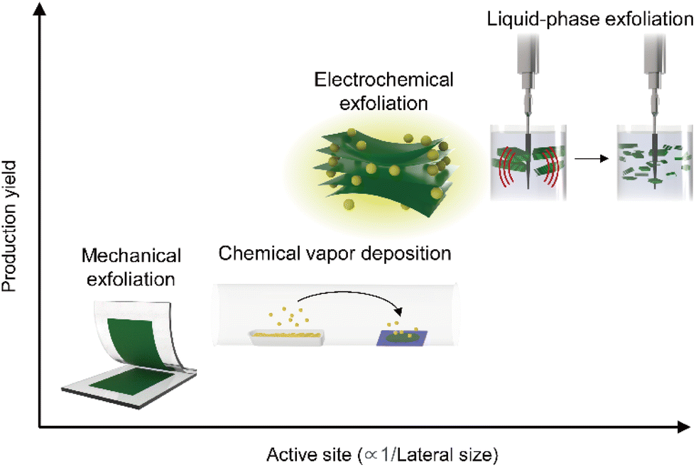 | ||
| Fig. 2 Plot comparing the production yields and relative catalytic active site densities of 2D materials produced by various synthesis methods. | ||
Demonstration and practical application of catalytic 2D materials
For decades, MoS2 has been attracting significant attention as a catalytic 2D semiconductor for HER due to its promising catalytic properties and cost-effectiveness.74 As the edge sites of MoS2 have been expected to be the active site of the electrochemical reaction, while the basal plane has been considered as electrochemically inert,45 it was first demonstrated through a microcell fabricated through selected-area lithography (Fig. 3a).14 To compare the HER performance of each basal plane and the edge sites of the CVD-grown monolayer MoS2, all samples except for the reaction area were covered with poly(methyl methacrylate)(PMMA), and only the designated area of the MoS2 single flakes was selectively reacted (Fig. 3b and c). As a result, the expected higher catalytic activity at the edge sites was experimentally demonstrated (Fig. 3c and d). | ||
| Fig. 3 (a) On-chip local probe measurement setup for investigating the HER activity of a single MoS2 flake. (b and c) Optical images of the chips for measuring the HER activities of the (b) ∼0.8 μm2 basal plane and (c) 0.3 μm2 basal plane and 0.8 μm edge. (d) Polarization curves of the monolayer MoS2 basal plane, both with and without edge active sites, in the context of the HER. Reproduced with permission from ref. 14 Copyright 2017 John Wiley and Sons. (e) Scheme of edge-terminated TMDC films with the layers aligned perpendicular to the substrate, maximally exposing the edges of the layers and the corresponding TEM image. Reproduced with permission from ref. 40 Copyright 2013 American Chemical Society. (f) Comparison plot of catalytic activity between flat and nanoscrolled TMDCs. Reproduced with permission from ref. 75 Copyright 2022 American Chemical Society. (g) Synthesis processes of various morphologies. Reproduced with permission from ref. 76 Copyright 2022 John Wiley and Sons. (h) SEM image of the bulk MoS2 powder and photos of (i) MoS2 dispersion with a volume of 60 liters, (j) bare Cu foam and (k) the MoS2-based catalyst loaded on Cu foam. Reproduced with permission from ref. 77 Copyright 2020 Springer Nature. | ||
Therefore, many attempts have been further made to maximize the active site densities of MoS2, which has potentially comparable catalytic performances to noble metals. Most intuitively, an interesting approach has been reported that grows MoS2 as vertically aligned layers to expose highly dense edge sites (Fig. 3e).40 Furthermore, HER performances can be improved by applying thermal strain to induce more cracks and kinks to the CVD-grown MoS2 with a controlled cooling rate.75 It was also observed that when the rolling-up process was accelerated through liquid intercalation at the crack site, it was reconstructed into a nanoscroll and greatly improves the electrochemical reaction rate (Fig. 3f). Morphological approaches through the modification of synthetic methods were also considered, successfully yielding a variety of morphologies, including nanoparticles, nanoflowers, nanospheres, nanohollows, and oxide composites via a facile route hydrothermal process employing different solutions (Fig. 3g).76 These results suggest that structural differences in pure materials alone can lead to more promising electrocatalytic activities.
The excellent alternative with demonstrated potential can address the challenge of high-throughput scalable production for cost-effective, efficient, and durable electrocatalysts that perform well at high current densities required by industry. A uniform and stable catalyst plate can be achieved by applying a mass-produced MoS2-based ink onto square meter scale Cu foam, followed by thermal treatment (Fig. 3h–k).77 In addition to the cost-effectiveness, the production rate keeps increasing with subsequent developments of the exfoliation process, so it has huge potential as a catalyst for the next-generation electrochemical industry.
Modification to maximize the active sites of 2D materials
To address the significant challenge of limited active sites in 2D vdW materials, many approaches to modify the inactive basal plane have been proposed by introducing defects.78,79 The predominant method for enhancing activity involves etching and introducing a new element through doping can activate the otherwise inert basal plane. For example, MoS2 can undergo a top-down process to create edge sites on the basal plane through selective steam etching (Fig. 4a).80 The process is cascaded by varying the temperature of multilayer flakes, further increasing the density of active sites (Fig. 4b). The impact of etching was clearly demonstrated through microcell analysis (Fig. 4c and d) for precise measurement of HER performances. Consequently, as shown in Fig. 4e, the Tafel slope of etched MoS2 shows as low as approximately 100 mV dec−1, resulting in a significantly improved reaction rate mostly originated from the increased active sites. As revealed, point defects (e.g., vacancies) formed on the basal plane can serve as additional active sites, leading to the pursuit of defect engineering through a mild process rather than complete etching, such as low-energy plasma etching and electrodeposition of metal particles to induce vacancies.25,26,28Fig. 4f illustrates the overall process of maximizing vacancies by sequentially introducing metal electrodeposition following plasma etching.48 In the cases where a structure is challenging to etch vertically, vacancies can be formed through a solution process. An unstable and highly oxidizing solution, such as H2O2, can be employed for this purpose (Fig. 4g).81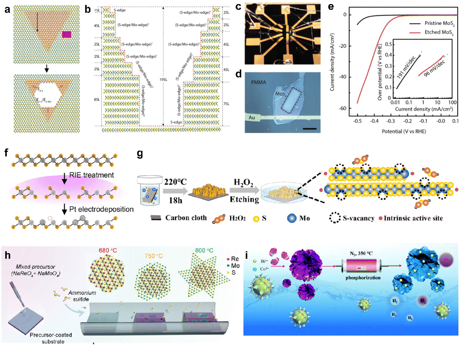 | ||
| Fig. 4 (a) Schematic of the evolution of hexagonal pits on two layers of MoS2. (b) Sectional schematic corresponding to (a). (c) Photo showing the electrochemical microcell. (d) Optical microscopy image of the microcell, revealing a window (indicated by the white dashed square) exposing the MoS2 basal plane. The scale bar is 20 μm. (e) Typical polarization curves measured from pristine and etched MoS2-based microcells in 0.5 M H2SO4 at a scan rate of 5 mV s−1, accompanied by the corresponding Tafel plot in the inset. Reproduced with permission from ref. 80 Copyright 2018 Elsevier. (f) Illustration of the RIE and electrochemical Pt deposition processes. Reproduced with permission from ref. 48 Copyright 2023 The Authors. (g) Schematic outlining the chemical etching process for introducing single S vacancies. Reproduced with permission from ref. 81 Copyright 2020 American Chemical Society. (h) Schematic illustration of the two-step CVD growth to synthesize the 1T′ RexMo1−xS2–2H MoS2 lateral heterostructure. Reproduced with permission from ref. 85 Copyright 2022 John Wiley and Sons. (i) Schematic illustrating the fabrication of Bi/CoP catalysts and a comparison of the HER energetic pathways between pristine CoP and Bi/CoP. Reproduced with permission from ref. 86 Copyright 2020 Royal Society of Chemistry. | ||
One of the primary challenges in surface defect engineering via etching is the issue of stability, often arising from the unstable flake state. Considering that the presence of chalcogen vacancies in 2D TMDCs can directly impact stability, it is noteworthy that interfaces within 2D materials, such as grain boundaries or homojunctions, exhibit imperfect lattice structures and improved chemical reactivity.82–84Fig. 4h illustrates a process of minimizing vacancies and creating an unstable lattice structure on the basal plane by introducing a third element during crystal synthesis via CVD.85 The resulting heterojunction flakes exhibit an average hydrogen adsorption free energy of nearly zero (0.26 eV), leading to a significant improvement in the catalyst performance. Furthermore, there are instances where the synthesis of intricate morphology structures, followed by doping, has been employed to maximize the desired effects.86–88 For instance, a 3D hierarchical CoP nanoflower, which was synthesized using the metal–organic framework self-sacrifice strategy, can be produced (Fig. 4i).86 Additionally, bismuth doping was introduced into the CoP nanoflower, synergistically optimizing the binding free energy of H adatoms on the CoP (202) facet and improving the HER performance. Based on such modification strategies, promising candidates that could genuinely replace noble metal catalysts are increasingly emerging.
2D materials as electrode layers
2D electrodes for loading catalysts: graphene
Graphene, with its high electrical conductivity and high surface area, plays a crucial role as a charge transfer pathway for HER catalysts such as 2D TMDCs and noble metals.89–91 Attempts to use high-quality large-area graphene to manufacture a catalytic electrode of a substantial wafer-scale start with finding an effective transfer method. Large-area single-layer graphene grown using CVD is primarily produced through the reaction of methane on copper or nickel (Ni) foil.67,92 Subsequently, the substrate needs to be removed and the graphene should be carefully positioned according to the desired location. Polymer-based dry or wet transfer methods have been developed and demonstrated utilizing materials such as PMMA,93 poly(bisphenol A carbonate),94,95 polystyrene,96 and thermal release tapes.97 Among these options, PMMA is the most widely employed due to its compatibility, light transparency, ease of handling, and adjustable viscosity.93,98,99 However, it is known that the polymer is not entirely removed during the transfer process, leaving behind the residue,100,101 which is detrimental for charge transfer characteristics that highly suppress the intrinsic characteristics of electrode materials. In addition to the surface contamination, water molecules and electrolyte ions can penetrate between graphene and base substrates, often through edges or small cracks in single-layer graphene during the HER. As the reaction begins and the hydrogen bubbles evolve, the graphene is supposedly separated from the substrate during the reaction.102,103Producing graphene electrodes for HER that are free from contamination and breakage can be approached in various ways. An improved transfer method, the flipped transfer technique, was developed by incorporating PMMA as an assisting adhesive layer (Fig. 5a).103 This method ensures the achievement of a pristine graphene surface free from polymer contaminants. Moreover, the hydrophobic PMMA layer sitting between the graphene electrode and the hydrophilic SiO2 substrate was optimized to enhance electrochemical reactions by preventing water infiltration and minimizing bubble-induced damage. This configuration is appropriate for electrochemical reactions, as the hydrophobic PMMA layer sitting between the graphene electrode and the hydrophilic SiO2 substrate prevents water intercalation and eliminates bubble-related damage.
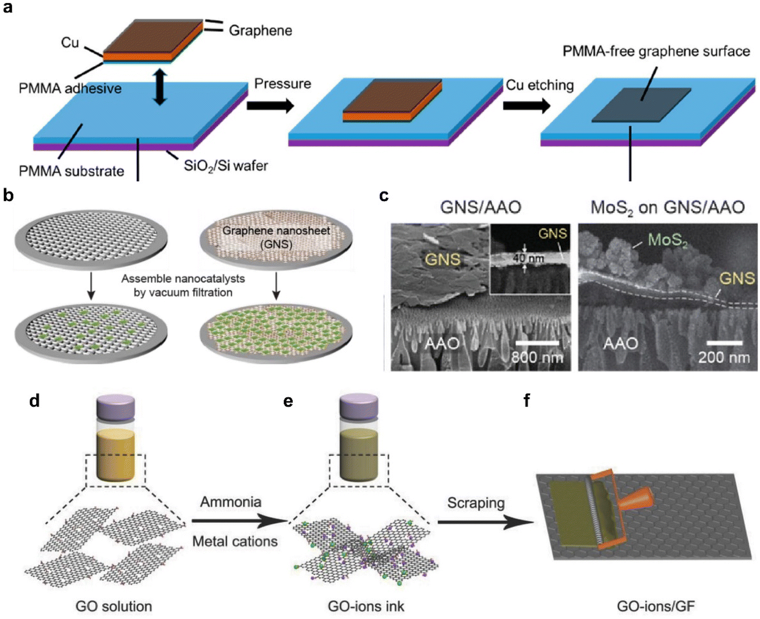 | ||
| Fig. 5 (a) Schematic illustration of the PMMA-assisted flipped transfer method. In contrast to conventional transfer methods, PMMA is employed as a substrate instead of a sacrificial layer. Reproduced with permission from ref. 103 Copyright 2017 American Chemical Society. (b) Schematic of the graphene nanosheet (GNS)-assisted approach for generating nanocatalyst electrodes. (c) SEM images of the GNS layer and the MoS2/GNS composite. Reproduced with permission from ref. 68 Copyright 2021 The Authors. (d) Dispersion of a graphene oxide (GO) solution. (e) Addition of ammonia and metal cations to create a GO ion ink. (f) Application of the GO ion ink to the surface of a graphite foil using an automatic film applicator. Reproduced with permission from ref. 114 Copyright 2018 John Wiley and Sons. | ||
For more practical applications of graphene, efforts have been made to produce large area films on a wafer-scale.104 Particularly, the solution-based process obtained from LPE has garnered significant interest.105,106 LPE is a top-down method suited for mass production and offers cost advantages through a low-temperature process. Using the resulting solution, graphene films can be prepared in various ways, including dip coating,107 drop casting,108 spin coating,109 spray coating,110 and inkjet printing.111,112Fig. 5b compares the effect of a graphene film as a filter for nano-size catalysts with a maximized surface area.68 The uniform film was fabricated by simple vacuum filtration without using a binder, thereby preventing problems represented by additional resistance in advance.113 The cross-section of the film with the catalyst vertically loaded clearly showed the separation of the graphene layer, which effectively acted as a filter (Fig. 5c). Facilitating the movement of electrons from graphene electrodes to catalysts through chemical bonding, rather than simple physical bonding, can be designed. This approach involves the induction of uniform adsorption of metal cations onto the modified graphene sheet through electrostatic attraction, leveraging the strong negative charge on the sheet's surface.114 (Fig. 5d–f) The method enables the production of a practical catalytic electrode utilizing almost 100% of the raw material. This strategy ensures excellent durability and thus provides a new platform for large-scale and high-yield production of graphene nanosheet-based electrocatalysts.
2D electrodes as templates for metallic catalyst growth
The efficiency of catalyst performance depends greatly on how the catalyst is loaded. Typically, catalysts are applied using ink-based preparation methods onto electrodes, which include drop casting,115,116 dip coating,117 and spray casting.116 Some methods involving atomic layer deposition and sputtering have also been suggested.118,119 However, ink-based methods often struggle to achieve a uniform thin film, often exhibiting issues like the coffee ring effect and aggregation.112,120 Ensuring proper adherence to substrates is another substantial challenge common to the above methods.121 Given these challenges, research has increasingly focused on cultivating catalysts that form a chemically robust bond with the electrode material, aiming to improve the efficiency. As shown in Fig. 5d–f, 2D vdW materials like graphene offer the advantage of strong and uniform adsorption, even at defect sites along the material's edges and basal plane.114 This characteristic makes these materials excellent templates for catalytic synthesis.Furthermore, HER catalysts can be directly synthesized on a conductive graphene electrode layer to minimize the contact resistance. In Fig. 6a, Ma et al. synthesized MoS2 on graphene to enhance conductivity for HER application and produced a binder-free, self-standing electrode.122 They synthesized MoS2 through a one-pot solvothermal method, which greatly lowered the reaction rate and succeeded in synthesizing flower-like complex structures. Catalytic metal nanoparticles can also be synthesized by electrodeposition.123,124Fig. 6b illustrates the synthesized Ni particles near defects in a graphene plane (Fig. 6c).124
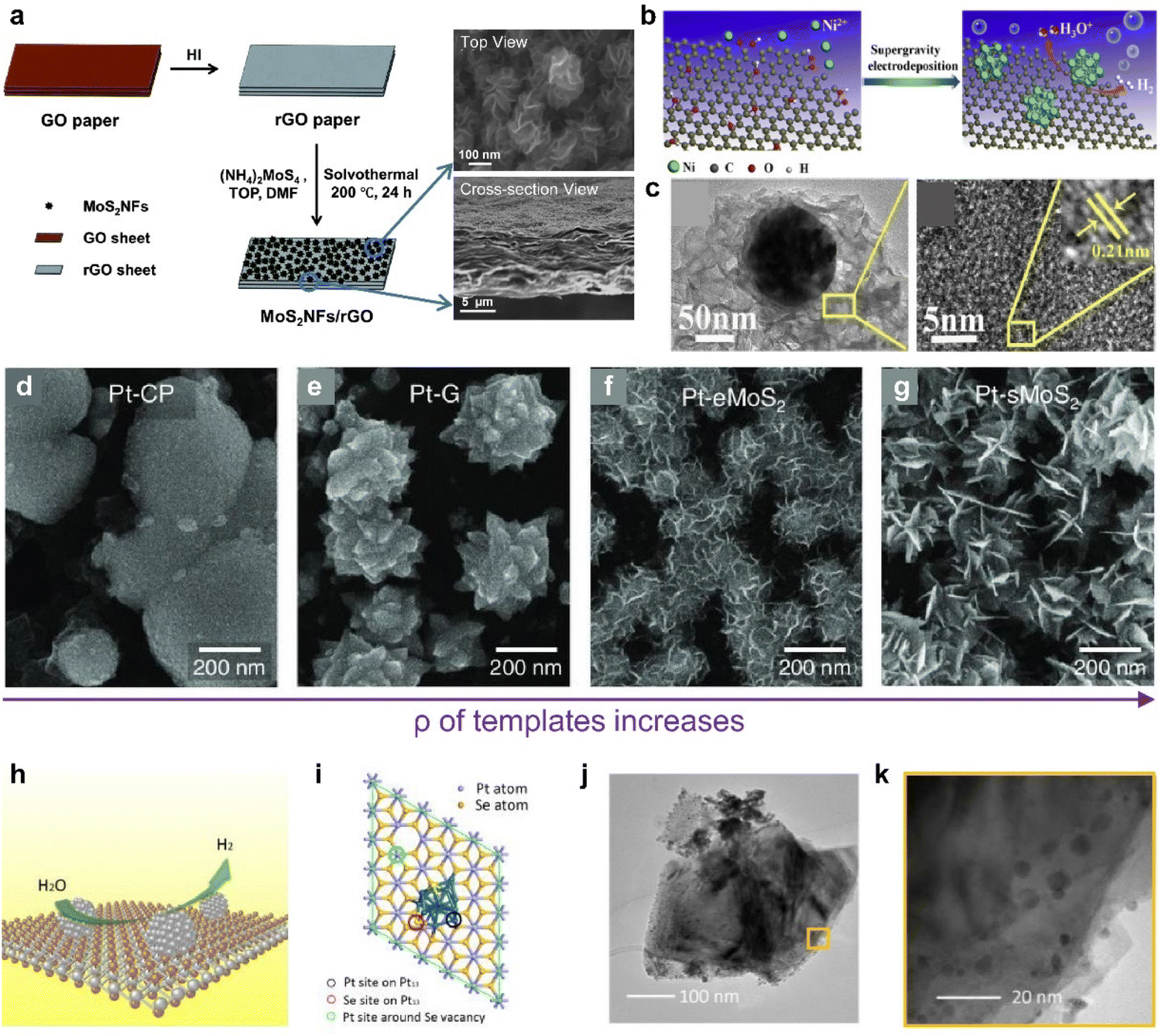 | ||
| Fig. 6 (a) Scheme of the MoS2NF/rGO paper fabrication process and SEM images illustrating the cross-section and top view of MoS2NF/rGO. Reproduced with permission from ref. 122 Copyright 2014 Royal Society of Chemistry. (b) Preparation process of the Ni–rGO catalyst. (c) TEM image of a single Ni particle supported on a rGO sheet and HRTEM images of the rGO sheet. The inset shows a closer view. Reproduced with permission from ref. 124 Copyright 2017 Elsevier. (d–g) Top-view SEM images of Pt nanoparticles grown on CP, graphene, eMoS2, and sMoS2 at 0.5 V. Reproduced with permission from ref. 33 Copyright 2022 The Authors. (h) Schematic representation of ultra-small Pt particles generated in situ on the surface of a PtSe2 nanosheet with Se vacancies. (i) The structural model used in density functional theory (DFT) calculations: a PtSe2 nanosheet decorated with a Pt13 cluster. Colored circles mark the active sites and Vn indicates the inclusion of n Se vacancies. (j) TEM images of PtSe2/Pt. (k) Magnified TEM image of PtSe2/Pt. Reproduced with permission from ref. 136 Copyright 2021 John Wiley and Sons. | ||
Furthermore, controlling the morphology123 of catalytic nanoparticles has been considered as an important goal to maximize electrocatalytically active sites and minimize coalescing hydrogen bubbles on the surface. The most critical factor influencing the morphology of particles is the reduction rate of metals.125,126 For the successful control over complex morphologies, it is imperative to maintain an extremely low reduction rate, necessitating prolonged reaction times during the overall nucleation and growth stages in this liquid-phase synthesis, which is based on homogeneous nucleation.127,128 To mitigate this challenge, the growth mechanism can be adjusted to manipulate the particle morphology by altering the reaction kinetics of Pt species through current modulation.129,130 In accordance with the diverse electrical properties of 2D materials, which structurally can serve as an electron carrier, the current flow to the surface can be regulated when employed as a template. In Fig. 6d–g, templates with various current levels were prepared and Pt particles were electrochemically deposited.33 Intriguingly, the shape and area density of the Pt nanoparticles exhibited significant variations depending on the growth template used. These template-dependent differences in the Pt nanoparticle morphology can be attributed to variations in the reduction rate of Pt ions for each template.129–131 Templates with higher resistance result in a slower reduction of Pt ions compared to the diffusion transport of the precursor, preventing the formation of a blank layer around the nucleus and maintaining an appropriate balance.129–131 Under such conditions, protrusions, such as edges or corners, are exposed to the precursor more than the particle core, promoting faster growth and leading to the formation of a flower-like structure.129–131 This groundbreaking strategy enables precise shape control through a brief electrochemical reaction and holds immense potential for various applications, as it can effectively maximize the catalyst's active surface area.
Lastly, 2D noble metal dichalcogenides (NMDs), which have attracted attention for their high carrier mobility and stability, can be another candidate for the strong interaction between particles and templates.132,133 For transition metal compounds, d-electrons define the phase structure and coordination environment, and the resulting interaction strength with active species.134 In particular, the d-band, which represents electron states associated with the d-orbitals of transition metals, exhibits better stability because it is highly occupied in NMDs, leading to strong metal adsorption on the surface.135 Pt, a representative catalyst for HER, can construct a heterointerface with PtSe2 through an electrochemical reduction method (Fig. 6h).136 At this time, it was found that a continuous Se vacancy was induced around the PtSe2/Pt boundary to strengthen the connection with particles (Fig. 6i). Large amounts of Pt particles at the edges of PtSe2 were observed, demonstrating the successful synthesis, and leading to good catalytic performance (Fig. 6j and k).
2D materials as interlayers
In recent studies, researchers have focused on exploring the interface layer between the catalyst and the electrode, which plays a crucial role in facilitating charge transfer between the catalyst and the electrode, while also imparting additional functionalities. One of the key factors under investigation is the Schottky barrier, which represents the tunnel barrier encountered by electrons at the interface between the semiconductor catalyst and the conductive support.137 This barrier can pose challenges to catalytic activity, primarily due to inefficient charge injection. From this standpoint, research has been conducted to accurately understand how interlayers influence the control of HER activity, considering the fact that adjacent support materials can alter various factors affecting the HER, such as ΔGH and the height of the Schottky barrier.137,138Fig. 7a shows a photograph of a microcell constructed using semi-metallic WTe2 as an interlayer between MoS2 and Au electrodes.139 Micromechanically-exfoliated flakes were stacked, and HER activities were elucidated to evaluate the influence of the interlayer without being affected by other factors. As a result, the relatively close Fermi level alignment between MoS2 and WTe2 resulted in a lower Schottky barrier, which could facilitate efficient electron injection to improve HER activity (Fig. 7b).137,138Fig. 7c shows that a perfectly stacked structure exhibits higher catalytic activity in common than a structure simply connected to MoS2 and WTe2, which emphasizes the need for an interlayer structure.139 | ||
| Fig. 7 (a) Optical image of the MoS2–WTe2 heterostructure. (b) Scheme of the MoS2–WTe2 heterostructure and the band alignment at the MoS2–WTe2 interface. (c) Comparison plot of overpotentials. Reproduced with permission from ref. 139 Copyright 2019 John Wiley and Sons. (d) Proposed mechanism for photocatalytic H2 evolution under visible light irradiation and the energy level for the EY–MoS2–TEOA system. Reproduced with permission from ref. 140 Copyright 2016 Royal Society of Chemistry. (e) Synthetic process of the MnCo–CH@NiFe–OH p–n junction. (f) Energy diagrams illustrating MnCo–CH and NiFe–OH (left) and the MnCo–CH@NiFe–OH p–n junction (right). Reproduced with permission from ref. 28 Copyright 2021 Elsevier. (g) STEM image of 3D nanoporous MoS2@rGO. (h) Schematic representation of MoS2@rGO. (i) Schematic illustration of band alignment and the mechanism of photoexcited charge transfer in MoS2@rGO. Reproduced with permission from ref. 144 Copyright 2018 American Chemical Society. | ||
In addition, Fig. 7d illustrates how electrons reach the HER reaction within the context of energy band alignment when an interlayer is introduced, also providing a potential applicability as a photocatalyst.50,140 The band energies of various 2D materials for water redox potentials have been extensively investigated, and 2D photocatalysts can be selected for water reduction or oxidation reactions based on valence band maximum (VBM) and conduction band minimum (CBM) locations.141 As depicted in Fig. 7e, the creation of a p–n junction structure is an essential process for implementing the photocatalyst.28 In the energy level diagram, p-type MnCo–CH possesses only the HER potential, while NiFe–OH features an overlapping energy level accommodating both electrons and the OER potential (Fig. 7f).28 When these two materials come into contact by forming a p–n junction, an adjustment in energy levels occurs, resulting in distinct catalytic behaviours for OER and HER within the hybrid structure (Fig. 7f). Electrons flow from NiFe–OH to MnCo–CH and recombine with holes until reaching Fermi level equilibrium, causing band bending.28 This bending increases the gap between NiFe–OH's valence band and the OER potential, facilitating electron flow and a positive charge on NiFe–OH, enhancing OH− movement and promoting the OER.28 Simultaneously, it widens the gap between MnCo–CH's conduction band and the HER potential, boosting electron mobility for H+ reduction to H2.28
Photocatalytic design can be realized using monolayer 2D materials.142,143 For instance, a heterojunction between p-type reduced graphene oxide (rGO) and n-type MoS2, synthesized via CVD, provides a suitable example (Fig. 7g).144 In this configuration, the CBM position of rGO is lower than that of MoS2, with the energy level of the HER situated below the CBM of MoS2. Consequently, this band alignment creates type-II (staggered) heterojunction structures that facilitate effective charge transfer upon photoexcitation. When exposed to visible light, electrons are excited from the VBM of rGO to the CBM. The designed CBM offset between MoS2 and rGO promotes efficient photoexcited electron transfer and facilitates the separation of holes and electrons, resulting in an electron-rich MoS2 layer conducive to the HER.144 Additionally, the photogenerated electrons contribute to a positive bias during the HER process, further enhancing the catalytic performance of the MoS2@rGO catalyst.144
Conclusions and outlook
Scalable synthesis of electrocatalytic-grade 2D materials with desired electronic properties to implement into catalytic electrodes by understanding the roles of each part including a catalytic layer, an electrode, and an interfacial layer can be an important first step towards enhancing the 2D material-based HER performance. Although considerable theoretical and empirical studies of 2D materials have been reported for their use in a catalytic layer and an electrode, investigations of interlayer applications remain relatively challenging due to the lack of appropriate processing methods for scalable p–n heterostructure formation. Heterostructures have shown the potential to enhance both the HER performance and functionality, but their accessibility has been limited by often involving sequential synthesis processes.28,145 However, the structural advantages of vertical stacking in 2D materials can be a key in addressing this issue. Furthermore, their wide range of electrical properties offers extensive choices for structure design based on energy bands. The excellence of 2D materials used as catalysts and electrode layers is summarized in Table 1. The HER performance of active sites in pristine 2D materials indicates the necessity of catalyst surface modification, and the modified catalysts exhibit outstanding characteristics. Furthermore, the adoption of graphene as an electrode layer is proven to be feasible by using Pt composites. However, due to the limited research on the role of functional 2D materials in enhancing the performance of catalytic electrodes as interlayers, only a few cases could be added. Improving synthesis and large-area film fabrication methods for effective vertical stacking can broaden the scope of functionality, ultimately leading to the development of more advanced 2D catalysts. This departure from the conventional paradigm focused on catalytic surfaces provides new insights into increasing catalytic activity in future research.| Sample | Synthesis method | Electrolyte | Overpotential | Tafel slope | Remark | Ref. |
|---|---|---|---|---|---|---|
| 2H-MoS2 basal plane | Chemical vapor deposition | 0.5 M H2SO4 | 425 mV(@10 mA cm−2) | 109 mV dec−1 | — | 14 |
| 2H-MoS2 Mo edge | Chemical vapor deposition | 0.5 M H2SO4 | 201 mV(@10 mA cm−2) | 68 mV dec−1 | Active site | |
| 2H-MoS2 on graphene | Liquid phase exfoliation | 1 M KOH | 486 mV(@10 mA cm−2) | 97 mV dec−1 | Wafer-scale/graphene electrode | 68 |
| 1T′-MoS2 basal plane | Chemical vapor deposition | 0.5 M H2SO4 | 356 mV(@10 mA cm−2) | 84 mV dec−1 | — | 14 |
| 1T′-MoS2 Mo edge | Chemical vapor deposition | 0.5 M H2SO4 | 77 mV(@10 mA cm−2) | 60 mV dec−1 | Active site | |
| 1H-MoS2 edge site | Chemical vapor deposition | 0.5 M H2SO4 | 940 mV(@30 mA cm−2) | 130 mV dec−1 | Active site | 80 |
| 1H-MoS2 terrace | Chemical vapor deposition | 0.5 M H2SO4 | 1060 mV(@30 mA cm−2) | 130 mV dec−1 | — | |
| WTe2 basal plane | Mechanical exfoliation | 0.5 M H2SO4 | 390 mV(@10 mA cm−2) | 141 mV dec−1 | — | 137 |
| WTe2 (010) edge | Mechanical exfoliation | 0.5 M H2SO4 | 350 mV(@10 mA cm−2) | 135 mV dec−1 | Active site | |
| WTe2 (100) edge | Mechanical exfoliation | 0.5 M H2SO4 | 320 mV(@10 mA cm−2) | 110 mV dec−1 | Active site | |
| PtSe2 | Solid-state synthesis | 1 M KOH | 294 mV(@10 mA cm−2) | 147 mV dec−1 | — | 136 |
| Pt on N-doped graphene | Sacrificial template method | 0.5 M H2SO4 | 30 mV(@10 mA cm−2) | 28 mV dec−1 | Graphene electrode | 23 |
| Single atom Pt on graphene | Microwave-assisted synthesis | 0.5 M H2SO4 | 12 mV(@10 mA cm−2) | 29 mV dec−1 | Graphene electrode | 24 |
| Pt-deposited MoS2 | Electrodeposition of Pt | 1 M KOH | 74 mV(@10 mA cm−2) | 53 mV dec−1 | Surface modification | 33 |
| Ni–rGO1.0/Ni foam | Supergravity electrodeposition | 1 M NaOH | 36 mV(@10 mA cm−2) | 77 mV dec−1 | Surface modification | 124 |
| Etched MoS2 basal plane | Steam vapor etched @700 °C | 0.5 M H2SO4 | 350 mV(@10 mA cm−2) | 96 mV dec−1 | Surface modification | 80 |
| Etched MoS2 nanosheets | Immersed in 5 mol L−1 H2O2 solution | 0.5 M H2SO4 | 131 mV(@10 mA cm−2) | 48 mV dec−1 | Surface modification | 81 |
| RIE-treated 1T-PtSe2 | Ar plasma treatment | 1 M KOH | 198 mV(@10 mA cm−2) | Surface modification | 48 | |
| Pt-deposited 1T-PtSe2 | Electrodeposition of Pt | 1 M KOH | 27 mV(@10 mA cm−2) | Surface modification | ||
| Pt/PtSe2 | Electrochemical reduction method | 1 M KOH | 42 mV(@10 mA cm−2) | 53 mV dec−1 | Surface modification | 136 |
| 2H-MoS2/WTe2 | 0.5 M H2SO4 | 150 mV(@10 mA cm−2) | 40 mV dec−1 | Heterostructure | 139 | |
| 1T′-RexMo1−xS2/2H-MoS2 | 0.5 M H2SO4 | 84 mV(@10 mA cm−2) | 58 mV dec−1 | Heterostructure | 85 |
Conflicts of interest
There are no conflicts to declare.Acknowledgements
This work was supported by a National Research Foundation of Korea (NRF) grant funded by the Korean Government (MSIT) (RS-2023-00208538 and RS-2023-00237308) and the Korea Basic Science Institute (KBSI) National Research Facilities and Equipment Center (NFEC) grant funded by the Korean Government (Ministry of Education) (2019R1A6C1010031).References
- M. S. Dresselhaus and I. L. Thomas, Nature, 2001, 414, 332–337 CrossRef CAS PubMed
.
- J. Zhang, Q. Zhang and X. Feng, Adv. Mater., 2019, 31, 1808167 CrossRef PubMed
- S. A. Vilekar, I. Fishtik and R. Datta, J. Electrochem. Soc., 2010, 157, B1040 CrossRef CAS
- H. Wang, Q. Yi, L. Gao, Y. Gao, T. Liu, Y.-B. Jiang, Y. Sun and G. Zou, Nanoscale, 2017, 9, 16342–16348 RSC
- L. Cao, N. Zhang, L. Feng, J. Huang, Y. Feng, W. Li, D. Yang and Q. Liu, Nanoscale, 2018, 10, 14272–14279 RSC
- J. K. Nørskov, T. Bligaard, A. Logadottir, J. R. Kitchin, J. G. Chen, S. Pandelov and U. Stimming, J. Electrochem. Soc., 2005, 152, J23 CrossRef
- L. M. Gandía, R. Oroz, A. Ursúa, P. Sanchis and P. M. Diéguez, Energy Fuels, 2007, 21, 1699–1706 CrossRef
- Q. Zhang and J. Guan, Adv. Funct. Mater., 2020, 30, 2000768 CrossRef CAS
- J. Wang, F. Xu, H. Jin, Y. Chen and Y. Wang, Adv. Mater., 2017, 29, 1605838 CrossRef PubMed
- G. Zhao, K. Rui, S. X. Dou and W. Sun, Adv. Funct. Mater., 2018, 28, 1803291 CrossRef
- H. Wang, W. Fu, X. Yang, Z. Huang, J. Li, H. Zhang and Y. Wang, J. Mater. Chem. A, 2020, 8, 6926–6956 RSC
- D. Voiry, J. Yang and M. Chhowalla, Adv. Mater., 2016, 28, 6197–6206 CrossRef CAS PubMed
- G. Gao, A. P. O'Mullane and A. Du, ACS Catal., 2017, 7, 494–500 CrossRef CAS
- J. Zhang, J. Wu, H. Guo, W. Chen, J. Yuan, U. Martinez, G. Gupta, A. Mohite, P. M. Ajayan and J. Lou, Adv. Mater., 2017, 29, 1701955 CrossRef PubMed
- Z. Liu, K. Suenaga, P. J. F. Harris and S. Iijima, Phys. Rev. Lett., 2009, 102, 015501 CrossRef PubMed
- M. D. Siao, W. C. Shen, R. S. Chen, Z. W. Chang, M. C. Shih, Y. P. Chiu and C. M. Cheng, Nat. Commun., 2018, 9, 1442 CrossRef CAS PubMed
- L. Liu and T. Zhai, InfoMat, 2021, 3, 3–21 CrossRef CAS
- Y. Liu, Y. Huang and X. Duan, Nature, 2019, 567, 323–333 CrossRef CAS PubMed
- K. Choi, Y. T. Lee and S. Im, Nano Today, 2016, 11, 626–643 CrossRef CAS
- Z. Lin, Y. Liu, U. Halim, M. Ding, Y. Liu, Y. Wang, C. Jia, P. Chen, X. Duan, C. Wang, F. Song, M. Li, C. Wan, Y. Huang and X. Duan, Nature, 2018, 562, 254–258 CrossRef CAS PubMed
- J. Kim, O. Song, Y. S. Cho, M. Jung, D. Rhee and J. Kang, ACS Mater. Au, 2022, 2, 382–393 CrossRef CAS PubMed
- X. Chia and M. Pumera, Nat. Catal., 2018, 1, 909–921 CrossRef CAS
- B. Jiang, F. Liao, Y. Sun, Y. Cheng and M. Shao, Nanoscale, 2017, 9, 10138–10144 RSC
- S. Ye, F. Luo, Q. Zhang, P. Zhang, T. Xu, Q. Wang, D. He, L. Guo, Y. Zhang, C. He, X. Ouyang, M. Gu, J. Liu and X. Sun, Energy Environ. Sci., 2019, 12, 1000–1007 RSC
- L.-J. Ma and H. Shen, Appl. Surf. Sci., 2021, 545, 149013 CrossRef CAS
- X. Ping, D. Liang, Y. Wu, X. Yan, S. Zhou, D. Hu, X. Pan, P. Lu and L. Jiao, Nano Lett., 2021, 21, 3857–3863 CrossRef CAS PubMed
- A. K. Geim and I. V. Grigorieva, Nature, 2013, 499, 419–425 CrossRef CAS PubMed
- Y. Zeng, Z. Cao, J. Liao, H. Liang, B. Wei, X. Xu, H. Xu, J. Zheng, W. Zhu, L. Cavallo and Z. Wang, Appl. Catal., B, 2021, 292, 120160 CrossRef CAS
- Y. Liu, N. O. Weiss, X. Duan, H.-C. Cheng, Y. Huang and X. Duan, Nat. Rev. Mater., 2016, 1, 16042 CrossRef CAS
- B. Hinnemann, P. G. Moses, J. Bonde, K. P. Jørgensen, J. H. Nielsen, S. Horch, I. Chorkendorff and J. K. Nørskov, J. Am. Chem. Soc., 2005, 127, 5308–5309 CrossRef CAS PubMed
- Q. Tang and D.-E. Jiang, ACS Catal., 2016, 6, 4953–4961 CrossRef CAS
- J. Pan, R. Wang, X. Xu, J. Hu and L. Ma, Nanoscale, 2019, 11, 10402–10409 RSC
- Y. S. Cho, D. Rhee, J. Eom, J. Kim, M. Jung, Y. Son, Y.-K. Han, K. K. Kim and J. Kang, Small Sci., 2022, 2, 2200043 CrossRef CAS
- W. Yang and S. Chen, Chem. Eng. J., 2020, 393, 124726 CrossRef CAS
- D. Voiry, H. S. Shin, K. P. Loh and M. Chhowalla, Nat. Rev. Chem., 2018, 2, 0105 CrossRef CAS
- Z. Li, N. H. Attanayake, J. L. Blackburn and E. M. Miller, Energy Environ. Sci., 2021, 14, 6242–6286 RSC
- W. Sheng, M. Myint, J. G. Chen and Y. Yan, Energy Environ. Sci., 2013, 6, 1509–1512 RSC
- I. T. McCrum and M. T. M. Koper, Nat. Energy, 2020, 5, 891–899 CrossRef CAS
-
P. Sabatier, in La catalyse en chimie organique, ed. C. Béranger, 1920 Search PubMed
- D. Kong, H. Wang, J. J. Cha, M. Pasta, K. J. Koski, J. Yao and Y. Cui, Nano Lett., 2013, 13, 1341–1347 CrossRef CAS PubMed
- D. Voiry, H. Yamaguchi, J. Li, R. Silva, D. C. B. Alves, T. Fujita, M. Chen, T. Asefa, V. B. Shenoy, G. Eda and M. Chhowalla, Nat. Mater., 2013, 12, 850–855 CrossRef CAS PubMed
- W. Chen, E. J. G. Santos, W. Zhu, E. Kaxiras and Z. Zhang, Nano Lett., 2013, 13, 509–514 CrossRef CAS PubMed
- M. Zhuang, Y. Ding, X. Ou and Z. Luo, Nanoscale, 2017, 9, 4652–4659 RSC
- Y. Takahashi, Y. Kobayashi, Z. Wang, Y. Ito, M. Ota, H. Ida, A. Kumatani, K. Miyazawa, T. Fujita, H. Shiku, Y. E. Korchev, Y. Miyata, T. Fukuma, M. Chen and T. Matsue, Angew. Chem., Int. Ed., 2020, 59, 3601–3608 CrossRef CAS PubMed
- T. F. Jaramillo, K. P. Jørgensen, J. Bonde, J. H. Nielsen, S. Horch and I. Chorkendorff, Science, 2007, 317, 100–102 CrossRef CAS PubMed
- A. Chaves, J. G. Azadani, H. Alsalman, D. R. da Costa, R. Frisenda, A. J. Chaves, S. H. Song, Y. D. Kim, D. He, J. Zhou, A. Castellanos-Gomez, F. M. Peeters, Z. Liu, C. L. Hinkle, S.-H. Oh, P. D. Ye, S. J. Koester, Y. H. Lee, P. Avouris, X. Wang and T. Low, npj 2D Mater. Appl., 2020, 4, 29 CrossRef CAS
- Y. Niu, S. Gonzalez-Abad, R. Frisenda, P. Marauhn, M. Drüppel, P. Gant, R. Schmidt, N. S. Taghavi, D. Barcons, A. J. Molina-Mendoza, S. M. De Vasconcellos, R. Bratschitsch, D. Perez De Lara, M. Rohlfing and A. Castellanos-Gomez, Nanomaterials, 2018, 8, 725 CrossRef PubMed
- Y. S. Cho, D. Rhee, J. Lee, S. Y. Jung, J. Eom, V. Mazanek, B. Wu, T. Kang, S. Baek, H. Choi, Z. Sofer, S. Lee and J. Kang, EcoMat, 2023, 5, e12358 CrossRef CAS
- H. L. Zhuang and R. G. Hennig, J. Phys. Chem. C, 2013, 117, 20440–20445 CrossRef CAS
- K. Pramoda and C. N. R. Rao, ChemNanoMat, 2022, 8, e202200153 CrossRef CAS
- R. Tao, X. Li, X. Li, C. Shao and Y. Liu, Nanoscale, 2020, 12, 8320–8329 RSC
- J. Wang, Z. Guan, J. Huang, Q. Li and J. Yang, J. Mater. Chem. A, 2014, 2, 7960–7966 RSC
- K.-W. Park and A. M. Kolpak, J. Mater. Chem. A, 2019, 7, 6708–6719 RSC
- X. Huang, Z. Zeng, Z. Fan, J. Liu and H. Zhang, Adv. Mater., 2012, 24, 5979–6004 CrossRef CAS PubMed
- B. Lyu, M. Kim, H. Jing, J. Kang, C. Qian, S. Lee and J. H. Cho, ACS Nano, 2019, 13, 11392–11400 CrossRef CAS PubMed
- X. Zhang, J. Hu, Y. Cheng, H. Y. Yang, Y. Yao and S. A. Yang, Nanoscale, 2016, 8, 15340–15347 RSC
- Z. Lin, Y. Huang and X. Duan, Nat. Electron., 2019, 2, 378–388 CrossRef
- M. Velický and P. S. Toth, Appl. Mater. Today, 2017, 8, 68–103 CrossRef
- J.-H. Chen, C. Jang, S. Xiao, M. Ishigami and M. S. Fuhrer, Nat. Nanotechnol., 2008, 3, 206–209 CrossRef CAS PubMed
-
R. A. Serway and J. W. Jewett, Principles of physics, 1998 Search PubMed
- R. A. Matula, J. Phys. Chem. Ref. Data, 1979, 8, 1147–1298 CrossRef CAS
- J. Zhang, N. Kong, S. Uzun, A. Levitt, S. Seyedin, P. A. Lynch, S. Qin, M. Han, W. Yang, J. Liu, X. Wang, Y. Gogotsi and J. M. Razal, Adv. Mater., 2020, 32, 2001093 CrossRef CAS PubMed
- Y. Zhao, J. Qiao, Z. Yu, P. Yu, K. Xu, S. P. Lau, W. Zhou, Z. Liu, X. Wang, W. Ji and Y. Chai, Adv. Mater., 2017, 29, 1604230 CrossRef PubMed
- K. S. Novoselov, A. K. Geim, S. V. Morozov, D. Jiang, Y. Zhang, S. V. Dubonos, I. V. Grigorieva and A. A. Firsov, Science, 2004, 306, 666–669 CrossRef CAS PubMed
- H. Li, J. Wu, Z. Yin and H. Zhang, Acc. Chem. Res., 2014, 47, 1067–1075 CrossRef CAS PubMed
- J. Yang and H. S. Shin, J. Mater. Chem. A, 2014, 2, 5979–5985 RSC
- K. S. Kim, Y. Zhao, H. Jang, S. Y. Lee, J. M. Kim, K. S. Kim, J.-H. Ahn, P. Kim, J.-Y. Choi and B. H. Hong, Nature, 2009, 457, 706–710 CrossRef CAS PubMed
- Y. S. Cho, D. Rhee, H. J. Kim, H. S. Kim, J. M. Baik and J. Kang, Adv. Mater. Interfaces, 2021, 8, 2101576 CrossRef CAS
- N. Cheng, S. Stambula, D. Wang, M. N. Banis, J. Liu, A. Riese, B. Xiao, R. Li, T.-K. Sham, L.-M. Liu, G. A. Botton and X. Sun, Nat. Commun., 2016, 7, 13638 CrossRef CAS PubMed
- K. S. Novoselov, V. I. Fal'ko, L. Colombo, P. R. Gellert, M. G. Schwab and K. Kim, Nature, 2012, 490, 192–200 CrossRef CAS PubMed
- L. Li, Z. Qin, L. Ries, S. Hong, T. Michel, J. Yang, C. Salameh, M. Bechelany, P. Miele, D. Kaplan, M. Chhowalla and D. Voiry, ACS Nano, 2019, 13, 6824–6834 CrossRef CAS PubMed
- J. Kim, S. Kim, Y. S. Cho, M. Choi, S.-H. Jung, J. H. Cho, D. Whang and J. Kang, ACS Appl. Mater. Interfaces, 2021, 13, 12221–12229 CrossRef CAS PubMed
- G. Eda, H. Yamaguchi, D. Voiry, T. Fujita, M. Chen and M. Chhowalla, Nano Lett., 2011, 11, 5111–5116 CrossRef CAS PubMed
- W. Jaegermann and H. Tributsch, Prog. Surf. Sci., 1988, 29, 1–167 CrossRef CAS
- R. Ghosh, M. Singh, L. W. Chang, H.-I. Lin, Y. S. Chen, J. Muthu, B. Papnai, Y. S. Kang, Y.-M. Liao and K. P. Bera, ACS Nano, 2022, 16, 5743–5751 CrossRef CAS PubMed
- T. Van Nguyen, M. Tekalgne, T. P. Nguyen, W. Wang, S. H. Hong, J. H. Cho, Q. van Le, H. W. Jang, S. H. Ahn and S. Y. Kim, Int. J. Energy Res., 2022, 46, 11479–11491 CrossRef CAS
- C. Zhang, Y. Luo, J. Tan, Q. Yu, F. Yang, Z. Zhang, L. Yang, H.-M. Cheng and B. Liu, Nat. Commun., 2020, 11, 3724 CrossRef CAS PubMed
- J. Xie, X. Yang and Y. Xie, Nanoscale, 2020, 12, 4283–4294 RSC
- H. Zhang and R. Lv, J. Materiomics, 2018, 4, 95–107 CrossRef
- Z. Wang, Q. Li, H. Xu, C. Dahl-Petersen, Q. Yang, D. Cheng, D. Cao, F. Besenbacher, J. V. Lauritsen, S. Helveg and M. Dong, Nano Energy, 2018, 49, 634–643 CrossRef CAS
- X. Wang, Y. Zhang, H. Si, Q. Zhang, J. Wu, L. Gao, X. Wei, Y. Sun, Q. Liao, Z. Zhang, K. Ammarah, L. Gu, Z. Kang and Y. Zhang, J. Am. Chem. Soc., 2020, 142, 4298–4308 CrossRef CAS PubMed
- Y. He, P. Tang, Z. Hu, Q. He, C. Zhu, L. Wang, Q. Zeng, P. Golani, G. Gao, W. Fu, Z. Huang, C. Gao, J. Xia, X. Wang, X. Wang, C. Zhu, Q. M. Ramasse, A. Zhang, B. An, Y. Zhang, S. Martí-Sánchez, J. R. Morante, L. Wang, B. K. Tay, B. I. Yakobson, A. Trampert, H. Zhang, M. Wu, Q. J. Wang, J. Arbiol and Z. Liu, Nat. Commun., 2020, 11, 57 CrossRef CAS PubMed
- Y. Chen, P. Ou, X. Bie and J. Song, J. Mater. Chem. A, 2020, 8, 19522–19532 RSC
- R. Song, D. Li, Y. Xu, J. Gao, L. Wang and Y. Li, Nanoscale Adv., 2022, 4, 865–870 RSC
- H. T. T. Nguyen, L. A. Adofo, S.-H. Yang, H.-J. Kim, S. H. Choi, B. Kirubasankar, B. W. Cho, A. Ben-Smith, J. Kang, Y.-M. Kim, S. M. Kim, Y.-K. Han and K. K. Kim, Adv. Funct. Mater., 2023, 33, 2209572 CrossRef CAS
- L. Guo, X. Bai, H. Xue, J. Sun, T. Song, S. Zhang, L. Qin, K. Huang, F. He and Q. Wang, Chem. Commun., 2020, 56, 7702–7705 RSC
- Z. Hu, L. Zhang, J. Huang, Z. Feng, Q. Xiong, Z. Ye, Z. Chen, X. Li and Z. Yu, Nanoscale, 2021, 13, 8264–8274 RSC
- A. Nano LettersHasani, T. P. Nguyen, M. Tekalgne, Q. Van Le, K. S. Choi, T. H. Lee, T. Jung Park, H. W. Jang and S. Y. Kim, Appl. Catal., A, 2018, 567, 73–79 CrossRef
- Y. Li, H. Wang, L. Xie, Y. Liang, G. Hong and H. Dai, J. Am. Chem. Soc., 2011, 133, 7296–7299 CrossRef CAS PubMed
- S. Chen, J. Duan, M. Jaroniec and S. Z. Qiao, Angew. Chem., Int. Ed., 2013, 52, 13567–13570 CrossRef CAS PubMed
- D. H. Youn, S. Han, J. Y. Kim, J. Y. Kim, H. Park, S. H. Choi and J. S. Lee, ACS Nano, 2014, 8, 5164–5173 CrossRef CAS PubMed
- X. Li, C. W. Magnuson, A. Venugopal, R. M. Tromp, J. B. Hannon, E. M. Vogel, L. Colombo and R. S. Ruoff, J. Am. Chem. Soc., 2011, 133, 2816–2819 CrossRef CAS PubMed
- X. Liang, B. A. Sperling, I. Calizo, G. Cheng, C. A. Hacker, Q. Zhang, Y. Obeng, K. Yan, H. Peng, Q. Li, X. Zhu, H. Yuan, A. R. Hight Walker, Z. Liu, L.-M. Peng and C. A. Richter, ACS Nano, 2011, 5, 9144–9153 CrossRef PubMed
- H. J. Park, J. Meyer, S. Roth and V. Skákalová, Carbon, 2010, 48, 1088–1094 CrossRef CAS
- Y.-C. Lin, C. Jin, J.-C. Lee, S.-F. Jen, K. Suenaga and P.-W. Chiu, ACS Nano, 2011, 5, 2362–2368 CrossRef CAS PubMed
- E. H. Lock, M. Baraket, M. Laskoski, S. P. Mulvaney, W. K. Lee, P. E. Sheehan, D. R. Hines, J. T. Robinson, J. Tosado, M. S. Fuhrer, S. C. Hernández and S. G. Walton, Nano Lett., 2012, 12, 102–107 CrossRef CAS PubMed
- J. D. Caldwell, T. J. Anderson, J. C. Culbertson, G. G. Jernigan, K. D. Hobart, F. J. Kub, M. J. Tadjer, J. L. Tedesco, J. K. Hite, M. A. Mastro, R. L. Myers-Ward, C. R. Eddy Jr., P. M. Campbell and D. K. Gaskill, ACS Nano, 2010, 4, 1108–1114 CrossRef CAS PubMed
- J. Kang, D. Shin, S. Bae and B. H. Hong, Nanoscale, 2012, 4, 5527–5537 RSC
- M. Her, R. Beams and L. Novotny, Phys. Lett. A, 2013, 377, 1455–1458 CrossRef CAS
- C. Gong, H. C. Floresca, D. Hinojos, S. McDonnell, X. Qin, Y. Hao, S. Jandhyala, G. Mordi, J. Kim, L. Colombo, R. S. Ruoff, M. J. Kim, K. Cho, R. M. Wallace and Y. J. Chabal, J. Phys. Chem. C, 2013, 117, 23000–23008 CrossRef CAS
- Y.-C. Lin, C.-C. Lu, C.-H. Yeh, C. Jin, K. Suenaga and P.-W. Chiu, Nano Lett., 2012, 12, 414–419 CrossRef CAS PubMed
- S. Yasuda, K. Tamura, T.-O. Terasawa, M. Yano, H. Nakajima, T. Morimoto, T. Okazaki, R. Agari, Y. Takahashi, M. Kato, I. Yagi and H. Asaoka, J. Phys. Chem. C, 2020, 124, 5300–5307 CrossRef CAS
- A. Xie, N. Xuan, K. Ba and Z. Sun, ACS Appl. Mater. Interfaces, 2017, 9, 4643–4648 CrossRef CAS PubMed
- Y. Lee, S. Bae, H. Jang, S. Jang, S.-E. Zhu, S. H. Sim, Y. I. Song, B. H. Hong and J.-H. Ahn, Nano Lett., 2010, 10, 490–493 CrossRef CAS PubMed
- Y. Hernandez, V. Nicolosi, M. Lotya, F. M. Blighe, Z. Sun, S. De, I. T. McGovern, B. Holland, M. Byrne, Y. K. Gun'Ko, J. J. Boland, P. Niraj, G. Duesberg, S. Krishnamurthy, R. Goodhue, J. Hutchison, V. Scardaci, A. C. Ferrari and J. N. Coleman, Nat. Nanotechnol., 2008, 3, 563–568 CrossRef CAS PubMed
- M. Lotya, Y. Hernandez, P. J. King, R. J. Smith, V. Nicolosi, L. S. Karlsson, F. M. Blighe, S. De, Z. Wang, I. T. McGovern, G. S. Duesberg and J. N. Coleman, J. Am. Chem. Soc., 2009, 131, 3611–3620 CrossRef CAS PubMed
- X. Wang, L. Zhi and K. Müllen, Nano Lett., 2008, 8, 323–327 CrossRef CAS PubMed
- C.-Y. Su, A.-Y. Lu, Y. Xu, F.-R. Chen, A. N. Khlobystov and L.-J. Li, ACS Nano, 2011, 5, 2332–2339 CrossRef CAS PubMed
- V. C. Tung, M. J. Allen, Y. Yang and R. B. Kaner, Nat. Nanotechnol., 2009, 4, 25–29 CrossRef CAS PubMed
- S. Gilje, S. Han, M. Wang, K. L. Wang and R. B. Kaner, Nano Lett., 2007, 7, 3394–3398 CrossRef CAS PubMed
- K.-Y. Shin, J.-Y. Hong and J. Jang, Chem. Commun., 2011, 47, 8527–8529 RSC
- O. Song, D. Rhee, J. Kim, Y. Jeon, V. Mazánek, A. Söll, Y. A. Kwon, J. H. Cho, Y.-H. Kim, Z. Sofer and J. Kang, npj 2D Mater. Appl., 2022, 6, 64 CrossRef CAS
- X. Yu, M. Zhang, J. Chen, Y. Li and G. Shi, Adv. Energy Mater., 2016, 6, 1501492 CrossRef
- X. Yu, M. Zhang, Y. Tong, C. Li and G. Shi, Adv. Energy Mater., 2018, 8, 1800403 CrossRef
- B. Seger and P. V. Kamat, J. Phys. Chem. C, 2009, 113, 7990–7995 CrossRef CAS
- H. Vrubel, D. Merki and X. Hu, Energy Environ. Sci., 2012, 5, 6136–6144 RSC
- H. W. Kim, M. B. Ross, N. Kornienko, L. Zhang, J. Guo, P. Yang and B. D. McCloskey, Nat. Catal., 2018, 1, 282–290 CrossRef
- J. An, Y.-B. Kim and F. B. Prinz, Phys. Chem. Chem. Phys., 2013, 15, 7520–7525 RSC
- D. Gruber, N. Ponath, J. Müller and F. Lindstaedt, J. Power Sources, 2005, 150, 67–72 CrossRef CAS
- H. Li, D. Buesen, R. Williams, J. Henig, S. Stapf, K. Mukherjee, E. Freier, W. Lubitz, M. Winkler, T. Happe and N. Plumeré, Chem. Sci., 2018, 9, 7596–7605 RSC
- M. S. Saha, A. F. Gullá, R. J. Allen and S. Mukerjee, Electrochim. Acta, 2006, 51, 4680–4692 CrossRef CAS
- C.-B. Ma, X. Qi, B. Chen, S. Bao, Z. Yin, X.-J. Wu, Z. Luo, J. Wei, H.-L. Zhang and H. Zhang, Nanoscale, 2014, 6, 5624–5629 RSC
- Y.-G. Huang, H.-L. Fan, Z.-K. Chen, C.-B. Gu, M.-X. Sun, H.-Q. Wang and Q.-Y. Li, Int. J. Hydrogen Energy, 2016, 41, 3786–3793 CrossRef CAS
- L. Wang, Y. Li, M. Xia, Z. Li, Z. Chen, Z. Ma, X. Qin and G. Shao, J. Power Sources, 2017, 347, 220–228 CrossRef CAS
- J. Chen, T. Herricks, M. Geissler and Y. Xia, J. Am. Chem. Soc., 2004, 126, 10854–10855 CrossRef CAS PubMed
- J. Chen, T. Herricks and Y. Xia, Angew. Chem., Int. Ed., 2005, 44, 2589–2592 CrossRef CAS PubMed
- S. H. Sun, D. Q. Yang, D. Villers, G. X. Zhang, E. Sacher and J. P. Dodelet, Adv. Mater., 2008, 20, 571–574 CrossRef CAS
- L. Lin, Z. Sun, M. Yuan, J. He, R. Long, H. Li, C. Nan, G. Sun and S. Ma, J. Mater. Chem. A, 2018, 6, 8068–8077 RSC
- G. J. Leong, M. C. Schulze, M. B. Strand, D. Maloney, S. L. Frisco, H. N. Dinh, B. Pivovar and R. M. Richards, Appl. Organomet. Chem., 2014, 28, 1–17 CrossRef CAS
- T. Yang, J. Liu, J. Dai and Y. Han, CrystEngComm, 2017, 19, 72–79 RSC
- T. Yang and Y. Han, Cryst. Growth Des., 2016, 16, 2850–2859 CrossRef CAS
- L. Pi, L. Li, K. Liu, Q. Zhang, H. Li and T. Zhai, Adv. Funct. Mater., 2019, 29, 1904932 CrossRef CAS
- Y. Zhou, J. Zhang, E. Song, J. Lin, J. Zhou, K. Suenaga, W. Zhou, Z. Liu, J. Liu, J. Lou and H. J. Fan, Nat. Commun., 2020, 11, 2253 CrossRef CAS PubMed
- Z. Wang, Z. Lin, J. Deng, S. Shen, F. Meng, J. Zhang, Q. Zhang, W. Zhong and L. Gu, Adv. Energy Mater., 2021, 11, 2003023 CrossRef CAS
- M.-W. Gu, H. H. Peng, I. W. P. Chen and C.-H. Chen, Nat. Mater., 2021, 20, 658–664 CrossRef CAS PubMed
- Z. Wang, B. Xiao, Z. Lin, Y. Xu, Y. Lin, F. Meng, Q. Zhang, L. Gu, B. Fang, S. Guo and W. Zhong, Angew. Chem., Int. Ed., 2021, 60, 23388–23393 CrossRef CAS PubMed
- Y. Zhou, J. L. Silva, J. M. Woods, J. V. Pondick, Q. Feng, Z. Liang, W. Liu, L. Lin, B. Deng, B. Brena, F. Xia, H. Peng, Z. Liu, H. Wang, C. M. Araujo and J. J. Cha, Adv. Mater., 2018, 30, 1706076 CrossRef PubMed
- D. Voiry, R. Fullon, J. Yang, C. de Carvalho Castro e Silva, R. Kappera, I. Bozkurt, D. Kaplan, M. J. Lagos, P. E. Batson, G. Gupta, A. D. Mohite, L. Dong, D. Er, V. B. Shenoy, T. Asefa and M. Chhowalla, Nat. Mater., 2016, 15, 1003–1009 CrossRef CAS PubMed
- Y. Zhou, J. V. Pondick, J. L. Silva, J. M. Woods, D. J. Hynek, G. Matthews, X. Shen, Q. Feng, W. Liu, Z. Lu, Z. Liang, B. Brena, Z. Cai, M. Wu, L. Jiao, S. Hu, H. Wang, C. M. Araujo and J. J. Cha, Small, 2019, 15, 1900078 CrossRef PubMed
- M. Yin, C. Wu, F. Jia, L. Wang, P. Zheng and Y. Fan, RSC Adv., 2016, 6, 75618–75625 RSC
- T. Su, Q. Shao, Z. Qin, Z. Guo and Z. Wu, ACS Catal., 2018, 8, 2253–2276 CrossRef CAS
- L. K. Putri, B.-J. Ng, W.-J. Ong, H. W. Lee, W. S. Chang and S.-P. Chai, J. Mater. Chem. A, 2018, 6, 3181–3194 RSC
- Y. Wang, Z. Ding, N. Arif, W.-C. Jiang and Y.-J. Zeng, Mater. Adv., 2022, 3, 3389–3417 RSC
- Y. Zhang, J. Du, Z. Wang, M. Luo, Y. Tian, T. Fujita, Q. Xue and M. Chen, ACS Appl. Energy Mater., 2018, 1, 2183–2191 CrossRef CAS
- C. Liu, T. Gong, J. Zhang, X. Zheng, J. Mao, H. Liu, Y. Li and Q. Hao, Appl. Catal., B, 2020, 262, 118245 CrossRef CAS
| This journal is © The Royal Society of Chemistry 2024 |