
Making coordination networks ionic: a unique strategy to achieve solution-processable hybrid semiconductors
Xiuze
Hei
ab and
Jing
Li
 *ba
*ba
aHoffmann Institute of Advanced Materials, Shenzhen Polytechnic, 7098 Liuxian Blvd, Nanshan District, Shenzhen, 518055, People's Republic of China. E-mail: jingli@rutgers.edu
bDepartment of Chemistry and Chemical Biology, Rutgers University, 123 Bevier Road, Piscataway, New Jersey 08854, USA
First published on 8th August 2023
Abstract
The development of high-performance, solution-processable semiconducting materials is crucial for the advancement of emerging clean-energy technologies such as light-emitting diodes and photovoltaics. While hybrid perovskites have shown considerable promise for implementation in these technologies, their reliance on toxic metals and relatively low stability towards moisture and chemical environments remain to be addressed. In this Chemistry Frontiers article, we describe a unique strategy to build nontoxic, robust and solution-processable hybrid semiconductors based on copper halide by incorporating ionic bonds in coordination complexes (molecular or extended network structures). Specifically, these compounds are made of anionic copper(I) halide and cationic organic ligands that form both coordinate and ionic bonds at the inorganic/organic interfaces and are referred to as all-in-one (AIO)-type structures. The unique bonding nature renders the AIO-type structures with greatly enhanced solubility, excellent optical tunability and remarkable framework stability, all highly desirable for thin-film based optoelectronic devices. We will highlight the most recent progress in the development of this material group, including their design strategies, important properties and potential for clean-energy related applications. We will also briefly discuss the existing challenges and future outlook of these materials.
Introduction
Crystalline inorganic–organic hybrid structures represent an important class of functional materials. Such materials consist of both inorganic and organic motifs and thus possess a wide range of intriguing properties, not only those intrinsic to each individual component but also new features extrinsic to both as a result of their synergetic interplay.1,2 Due to the extraordinary tunability of their structures and properties, crystalline inorganic–organic hybrid materials have been extensively investigated for various applications.3 Among them, high-performance solution-processable semiconductors suitable for emerging clean-energy related technologies such as light-emitting diodes (LEDs), and photovoltaics (PVs) have been one of the most targeted material classes.4,5Despite their superior optoelectronic properties, the utility of many conventional inorganic semiconductors in high-end thin-film based devices is often hampered due to their very poor solution processability. Designing new semiconducting materials that are solution-processable is critical for the device industries.6 Hybrid perovskites, an important class of crystalline inorganic–organic hybrid structures, represent a good example. Having excellent solubility in polar aprotic solvents, cost-effective and high-quality thin films of these materials can be fabricated via various solution processing methods, including screen printing, spin/spray coating, and inkjet printing.6,7 Optoelectronic devices (e.g. LEDs and PVs) based on hybrid perovskite thin-films have achieved competitive performance. Nevertheless, these materials suffer generally from their toxicity and instability.8,9 Though applaudable progress has been made to improve their stability, the search for alternative semiconductors that are nontoxic, robust, and solution-processable represents an important research objective, which may impact the field significantly.
Copper(I) halide (CuX, X = Cl, Br, I) based inorganic–organic hybrid semiconductors, especially those made of Cu–L (L = ligand) coordinate bonds, have attracted substantial interest in luminescence-related applications due to their numerous desired features including excellent structural/optical tunability, strong photoluminescence (PL), high resistance towards heat/moisture/chemical environment, and low cost, facile synthesis.10–12 However, the main issue that limits their applications, especially in optoelectronic devices, is their generally poor solubility. To address this issue, we have recently developed a new subclass of CuX based hybrid semiconductor materials, namely the all-in-one (AIO) type structures.13–15 The AIO-type structures differ from the CuX(L) family in that their inorganic motifs are not neutral CuX, but anionic (CumIm+n)n− and likewise, their organic ligands are not neutral L, but cationic Lk+. The inorganic anions and organic cations are further connected via Cu–L coordinate (dative) bonds to complete the bonding within the structure, as depicted in Fig. 1a. The unique multi-fold bonding at the inorganic/organic interface renders AIO-type structures with integrated properties from both coordinate bonds (e.g., structural/optical tunability, strong luminescence) and ionic bonds (e.g., solubility and stability), greatly raising their potential for applications in optoelectronic devices.
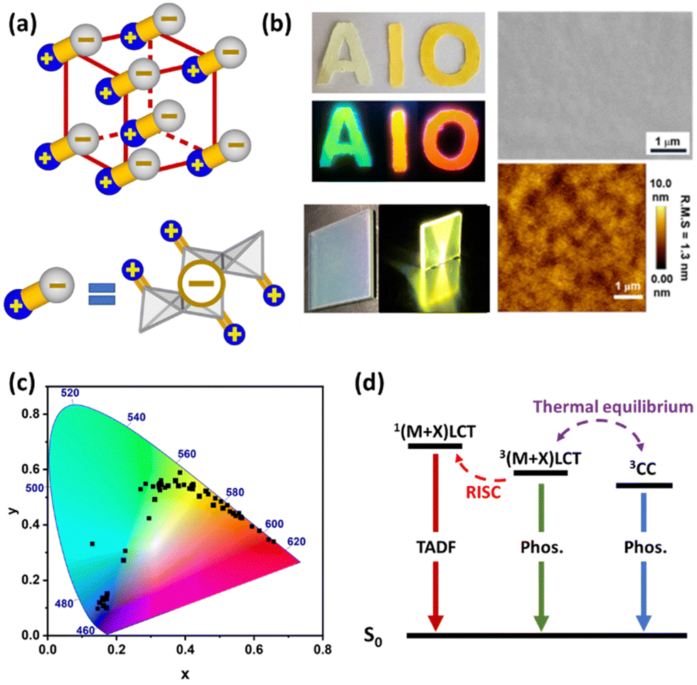 | ||
| Fig. 1 (a) Schematic illustration of AIO structures. Color scheme: blue: organic ligand; gray: inorganic motif; yellow rod: coordinate bond. Reproduced with permission from ref. 15 from the Royal Society of Chemistry. (b) Left: Selected AIO-type compounds coated on a soft fabric and glass substrate under daylight and UV light; Right: Top-view of the SEM (top) and AFM (bottom) image of the as-made thin film sample of a selected AIO compound. Reproduced with permission from ref. 13 and 18, from American Chemical Society. (c) Color chromaticity of all AIO-type compounds reported to date. (d) Schematic energy diagrams of different emission mechanisms of AIO compounds (Phos. = phosphorescence). | ||
Structures and physical properties
Synthesis and structures
To obtain a typical AIO structure, the ligand must be designed to contain (i) a cationic center to ensure the ionic interactions with the anionic inorganic motif, and (ii) available coordination sites to allow the subsequent formation of Cu–L dative bonds. The ionic feature of the ligand is generally realized by the alkylation of a tertiary amine or phosphine to yield a quaternary N or P cation that does not interfere with the coordination active sites. The active binding sites are typically N, P atoms that have strong coordination affinity towards Cu atoms. Besides the typical AIO structures, there are also structural variants inspired by the AIO approach. Examples include compounds made of coordinated CumXn(Lk) anions and free charge-balancing cations;16 as well as compounds containing [CuxIy]z− anions and Cu+ cations, separated in space by a Janus head ligand.17Since the success in systematic construction of the first group of the AIO-type structures in 2017,14 great efforts by us and others have been devoted to the design of new AIO structures and 60+ AIO compounds have been synthesized to date.13,14,16–26 Their structures range from molecular (zero-dimensional, 0D) species to one-dimensional (1D) chains and two-dimensional (2D) layers. A variety of inorganic anionic modules from the smallest CuI2− monomer to an infinite 2D network of Cu8I102− have been identified, revealing excellent structural diversity of this interesting material class. To gain insight into the ligand effects in these structures, which is crucial to guide the structure modification and property optimization, comprehensive studies have been carried out on different aspects, including coordination affinity,13,23 steric effect,20,22 connectivity19 and hybridization.21 The structure formation of AIO-type compounds may also be influenced by the synthesis conditions. By controlling the ratios of the reagents, different types of AIO structures may result even with the same ligand.
Various methods have been developed to grow high-quality single crystals of AIO-type compounds. The layered diffusion method is one of the most efficient approaches, wherein the reactants are dissolved in different solvents first and then transferred to a reaction vessel as two separated layers to allow slow diffusion to reduce the nucleation rate. In most cases, a middle buffer layer between the two reactant layers is used to further control the reaction rate. For the phases that require high temperatures, the solvothermal method is generally used, in which the solvent system plays an important role in the determination of the resulting structures. Additionally, this synthetic method sometimes involves in situ generation of the cationic ligands when alcohols are used as solvents, which can act as alkylating reagents at high temperatures.
Solution processability
Unlike most conventional coordinated networks of nD-CuX(L) (n = 1–3) that are insoluble in all common solvents,27,28 the AIO-type compounds demonstrate good to excellent solubility in polar aprotic solvents in most cases. Specifically, depending on the structure and composition their solubility in DMSO varies between 40 to 420 mg mL−1 at room temperature. For example, 420 mg of 1D-Cu4I6(bttmp)2 made of [Cu4I6]2− 1D chains can be readily dissolved in 1 mL of DMSO at room temperature, comparable to hybrid perovskites and inorganic salts.18,29,30 The extraordinary solubility of AIO compounds allows facile pin-hole-free thin-film fabrication by simple spin-coating methods (Fig. 1b), making their use possible in solution processed thin-film based optoelectronic devices.The intriguing solvation behavior of the AIO compounds has been studied in detail and the results suggest it is a direct result of introducing ionic bonds between neutral inorganic motifs (CuX) and organic ligands (L).13,20 Because of the unique bonding characteristics, the solvation of AIO compounds involves the structure complexation in DMSO to generate soluble small fragments, similar to those of hybrid perovskites.15,31,32 The dissolved species were identified as anionic CuX clusters which remain coordinated to the cationic ligands via dative bonds by NMR and mass spectrometry.20,21
Optical tenability
Compared to the CuX-based hybrid compounds made of pure ionic bonds, which are also well solution processable, the major advantage of the AIO compounds lies in their remarkable optical tunability.10 As shown in Fig. 1c, strong photoluminescence (with the highest internal quantum yield >90%)14,16–18 and emission maxima ranging from 430 nm to 630 nm have been achieved, covering the entire visible spectrum. In addition, our recent effort has successfully resulted in a number of AIO structures with low bandgaps of ∼1.3–1.7 eV. This further illustrates the potential of this intriguing material class for NIR emission related applications and their optical tunability.In pure ionic CuX hybrid structures, as the organic cations are generally far away from the anionic inorganic motifs with only weak interactions, their photoluminescence is typically cluster-centered (CC) emission. As such, their optical properties are mainly determined by the inorganic modules with negligible ligand effect in most cases, making the fine tuning of electronic structures difficult.33 In contrast, having Cu–L dative bonds, the emission mechanisms of AIO compounds may include metal halide-to-ligand charge transfer [(M + X)LCT], CC and a combination of the two (Fig. 1d), with a strong dependence on the Cu⋯Cu distances (an indicator of cuprophilic interaction). These variables can be altered to suit different application needs.
Generally, ligands with aliphatic binding sites afford AIO structures with relatively short Cu⋯Cu distances (<2.80 Å, twice the vdW radius of Cu atom) and CC emission mechanism. On the other hand, AIO compounds composed of ligands with aromatic binding sites often have longer Cu⋯Cu distance and follow the (M + X)LCT emission mechanism. Electronic structure analysis shows that for this subgroup of structures, the valence band maximum (VBM) is populated mainly by the inorganic motifs, while the conduction band minimum (CBM) is primarily made of the lowest unoccupied molecular orbital (LUMO) of the ligands. Therefore, by selecting ligands with different functional groups (e.g., electron donating or electron withdrawing groups), their LUMO energies, and consequently the bandgap and emission energy of the resultant AIO structures, can be systematically tuned. Interestingly, when the Cu⋯Cu distances approach ∼2.80 Å, the two emission pathways 3CC and3(M + X)LCT may couple and both are responsible for the photoluminescence of the hybrid structures.19 As the higher laying excited state requires higher energy, its relative intensity can be varied by adjusting the excitation energy, including temperature and excitation wavelength, which is often associated with responsive color change of the compounds toward heat and excitation energy.
Moreover, AIO materials often exhibit efficient thermally activated delayed fluorescence (TADF), which is highly favored in harvesting excitons generated in LED devices.34 The extensive (M + X)LCT character of their excited states generally induces distinct spatial separations of the frontier orbitals, leading to relatively small exchange integrals and, consequently, small energy gaps ΔE(S1–T1) between the lowest singlet state S1 and the lowest triplet state T1.35 As a result, a fraction of the electrons can be thermally populated back to S1 from T1via reverse intersystem crossing (RISC) and then follow S1 to S0 radiative transition, benefitting the harvesting of generated singlet and triplet excitons.
Stability
To be suitable for real-world applications, semiconductor materials must possess high resistivity towards moisture, light, and heat. Compared to CuX hybrid structures composed of pure coordinate or ionic bonds at the inorganic/organic interfaces, the framework stability of AIO compounds is significantly enhanced as a result of the synergistic effect of both bond types. With only a few exceptions, most AIO structures are stable over 200 °C, with some exceeding 300 °C. Moreover, many AIO compounds demonstrate stable PL performance against thermal and photo stress. For example, the IQY values of 0D-Cu4I6(pr-ted)2 and 0D-Cu4I6(tpp)2(bttmm)2 remain over 90% of their initial values after being exposed to hot air at 100 °C or to continuous UV irradiation (365 nm) for 20 days without protection.14 In another example, the crystallinity of 1D-Cu4I6(bttmp)2 remained nearly the same after being submerged in water for 2000 h.18 Different approaches have been applied to further improve the stability of these compounds and proven to be successful. These approaches include: (1) using ligands with higher connectivity to form multidentate structures; (2) selecting ligands with electron rich N, P or S sites, which can form particularly strong coordination bonds with Cu atoms; and (3) building extended networks to increase structural rigidity.Applications
As discussed above, the strategy of incorporating both coordinate and ionic bonds in AIO structures serves as a general and powerful tool not only for the synthesis of very robust materials but also for the assembly of extended networks with greatly enhanced solubility. This enables thin-film fabrication of the AIO semiconductors by simple solution based processes, which are not possible to achieve for other types of CuX-based hybrids.The AIO materials were first tested as phosphors in phosphor-converted white LEDs (pc-WLEDs). Such WLEDs generate warm-white light by coating a blue LED chip with blue-excitable yellow phosphor or multiple (green-red) phosphors.36 As phosphors currently dominating the pc-WLED market are made of rare-earth elements (REEs), which not only are subject to the potential supply and cost risks, but also cause severe environmental impact,37 seeking eco-friendly and REE-free alternative phosphor materials would bring substantial benefits to society. The AIO materials stand out as promising candidates due to the advantages mentioned in the previous section, coupled with their easily scalable synthesis, earth-abundance, and excellent blue-excitability.13,14,23 Prototype LED bulbs using selected AIO compounds as phosphors have been assembled.14 The findings imply that the molecular motions of compounds can be suppressed by the use of multidentate ligands, which effectively reduce nonradiative decay and lead to enhancements in IQYs.
Using chiral cationic ligands, a series of hierarchically structured noncentrosymmetrical AIO materials have been successfully synthesized via a non-classical crystallization process involving nanocrystal nucleation, aggregation, oriented attachment and mesoscopic transformation (Fig. 2a). They show interesting circularly polarized luminescence (CPL).25 The chiral AIO polycrystals assemble at nano- and micro-scales and yield a significantly improved luminescence dissymmetry factor (glum) of 1.5![[thin space (1/6-em)]](https://www.rsc.org/images/entities/char_2009.gif) × 10−2 without significant loss of its photoluminescence quantum yield (PLQY). Interestingly, the chiroptical properties of these AIO aggerates strongly hinge on the position of the chiral centre in the ligand, which can substantially influence the interactions among chiral groups within the hierarchically structured polycrystals. These findings point to the possibility of using these compounds as efficient CPL active materials.
× 10−2 without significant loss of its photoluminescence quantum yield (PLQY). Interestingly, the chiroptical properties of these AIO aggerates strongly hinge on the position of the chiral centre in the ligand, which can substantially influence the interactions among chiral groups within the hierarchically structured polycrystals. These findings point to the possibility of using these compounds as efficient CPL active materials.
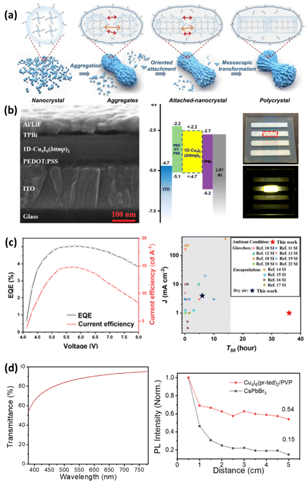 | ||
| Fig. 2 (a) Schematic illustration of the non-classical crystallization process of chiral AIO nanocrystals. Reproduced with permission from ref. 25 from Springer Nature. (b) Left to right: Cross-sectional HeIM image of the prototype YLED device structure using 1D-Cu4I6(bttmp)2 as the sole EML, overall energy band diagram and photographs of the fabricated device at “off” and “on” stages. (c) Left: EQE and current efficiency of the best-performing LED; right: T50 values of the yellow LED device and those of PeLEDs. (b) and (c) are reproduced with permission from ref. 18 from American Chemical Society. (d) Light transmittance (left) and light propagation property of the fabricated AIO based LSC film. Reproduced with permission from ref. 26 from American Chemical Society. | ||
Recently, we successfully demonstrated the use of AIO materials as an active emissive layer (EML).18 A first-ever yellow LED (YLED) device using an AIO-type hybrid semiconductor 1D-Cu4I6(bttmp)2 as the sole EML was fabricated (Fig. 2b). The spin-coated thin-film samples remain stable under harsh conditions (e.g., elevated temperature and high humidity) for over 2000 h without protection. The prototype YLED device achieves an external quantum efficiency (EQE) of 5.02%. Remarkably, the device demonstrates outstanding stability with its half-lifetime (T50) reaching 35.5 h under ambient conditions (Fig. 2c), while those of most hybrid perovskite-based LED devices are much shorter even tested under one form of protection (in a glovebox, under dry air or being encapsulated).38,39 This work certainly demonstrates the potential of AIO compounds for the construction of robust and nontoxic LED devices.
The possible use of AIO materials as luminescent solar concentrators (LSCs) was also investigated (Fig. 2d).26 LSCs are transparent waveguide substrates that help to provide higher optical concentration to the attached solar cells and thus increase their power output. The higher energy portion of the sunlight (at which the solar cell has low absorption) first gets absorbed by the luminescent material in LSC and converted to lower energy light, and the reemitted light then gets directed to the solar cell.40 A strongly luminescent film (9 cm × 4.5 cm) of 0D-AIO-Cu4I6(pr-ted)2/PVP (polyvinylpyrrolidone) was fabricated by facile blade coating to evaluate the performance of this AIO material as an LSC. The optimized film shows over 85% average transmittance in the visible light range and a high PLQY of 76.1%. In addition, it demonstrates much better waveguide properties than CsPbBr3. The good performance, coupled with their high stability, validates AIO materials as good candidates for LSCs.
Conclusions and outlook
As an emerging subclass of copper halide-based crystalline hybrid semiconductor, the AIO-type structures represent a new addition to the solution-processable material family that are critical for the future advancement of optoelectronic devices. They possess excellent air, moisture and thermal stability as a result of forming both strong coordinate and ionic bonds at the inorganic/organic interfaces. Their intriguing modular nature enables systematic control of the binding mode, metal–ligand connectivity, ligand orbital energies and consequently, the electronic structures and bandgaps, which, in turn, leads to fine-tuning of their chemical and physical properties to suit different application needs. Most remarkably, making the extended coordination networks ionic significantly enhances the solubility of the AIO-type compounds, taking them from totally insoluble to well soluble in polar aprotic solvents such as DMF and DMSO. Therefore, various cost-effective solution processing technologies can be used to fabricate high quality thin films of AIO-type semiconductors. These important and advantageous features offer considerable promise for their future use in clean energy related technologies. However, addressing the existing challenges and issues through further research and development is crucial to fully realize the potential of these materials.First of all, improving the performance and stability of the solution-processable blue-emitting LEDs (BLEDs), particularly deep blue-emitting LEDs, is of great interest to the lighting industry.41,42 The successful assembly of an ultrastable YLED device using the AIO compound as a sole EML may offer an alternative solution.18 To do so, robust and efficient AIO emitters (λem at ∼450 nm) with high photoluminescence and good charge transport properties need to be developed. In addition, the research on AIO compounds as the sole EML in LED devices is still in its infancy. Continuous and thorough investigations to further optimize and increase their EQE are vital to their ultimate implementation in general lighting technologies.
Secondly, the application of AIO semiconductors in the PV solar cells, one of the most important branches of optoelectronic devices, accounts for an important aspect of future research of these materials. Most recent work by us and others has yielded promising solution-processable low bandgap AIO compounds as efficient solar light absorbers. Although the photogenerated excitons may be somewhat localized due to the (M + X)LCT feature and can lead to low carrier mobility, a possible solution is to use ligands with strong π–π stackings to facilitate charge transfer.43 This is a very interesting new direction for the design of nontoxic and robust semiconductors targeted for PV solar cells.
Third, UV emissive AIO-type compounds represent an equally interesting subgroup but are yet to be synthesized. These materials will be extensively explored in our future studies.
Furthermore, building AIO compounds composed of high-dimensional inorganic modules is very desirable. Most of the AIO compounds reported to date contain inorganic modules limited to 0D clusters to 1D chains, with only a few exceptions of 2D layers. AIO structures with 3D inorganic backbones remain to be discovered. Increasing the dimensionality of inorganic motifs would, presumably, largely enhance/improve some very important properties directly relevant to device performance (e.g., conductivity, carrier mobility, diffusion length).
Finally, as a general tool for the design of solution processable and stable hybrid semiconductors, the strategy of including ionic bonds within coordinate networks can be extended to other hybrid materials44 beyond the copper halide-based hybrid family. By applying the AIO approach to other hybrid systems, exciting new opportunities for discovering advanced functional semiconductors could be unlocked.
Conflicts of interest
There are no conflicts to declare.Acknowledgements
Partial support from the U.S. Department of Energy (DOE), Office of Science, Office of Basic Energy Sciences under Award No. DE-SC0019902 is acknowledged.Notes and references
- B. Saparov and D. B. Mitzi, Organic–Inorganic Perovskites: Structural Versatility for Functional Materials Design, Chem. Rev., 2016, 116, 4558–4596 CrossRef CAS PubMed
.
- V. W.-W. Yam, V. K.-M. Au and S. Y.-L. Leung, Light-Emitting Self-Assembled Materials Based on d8 and d10 Transition Metal Complexes, Chem. Rev., 2015, 115, 7589–7728 CrossRef CAS PubMed
- H. Wang and D. H. Kim, Perovskite-based photodetectors: materials and devices, Chem. Soc. Rev., 2017, 46, 5204–5236 RSC
- P. Gao, M. Grätzel and M. K. Nazeeruddin, Organohalide lead perovskites for photovoltaic applications, Energy Environ. Sci., 2014, 7, 2448–2463 RSC
- M. D. Smith and H. I. Karunadasa, White-Light Emission from Layered Halide Perovskites, Acc. Chem. Res., 2018, 51, 619–627 CrossRef CAS PubMed
- P. Wang, Y. Wu, B. Cai, Q. Ma, X. Zheng and W.-H. Zhang, Solution-Processable Perovskite Solar Cells toward Commercialization: Progress and Challenges, Adv. Funct. Mater., 2019, 29, 1807661 CrossRef CAS
- F. Huang, M. Li, P. Siffalovic, G. Cao and J. Tian, From scalable solution fabrication of perovskite films towards commercialization of solar cells, Energy Environ. Sci., 2019, 12, 518–549 RSC
- G. Niu, W. Li, F. Meng, L. Wang, H. Dong and Y. Qiu, Study on the stability of CH3NH3PbI3 films and the effect of post-modification by aluminum oxide in all-solid-state hybrid solar cells, J. Mater. Chem. A, 2014, 2, 705–710 RSC
- Z. Fan, H. Xiao, Y. Wang, Z. Zhao, Z. Lin, H.-C. Cheng, S.-J. Lee, G. Wang, Z. Feng, W. A. Goddard, Y. Huang and X. Duan, Layer-by-Layer Degradation of Methylammonium Lead Tri-iodide Perovskite Microplates, Joule, 2017, 1, 548–562 CrossRef CAS
- W. Liu, Y. Fang and J. Li, Copper Iodide Based Hybrid Phosphors for Energy-Efficient General Lighting Technologies, Adv. Funct. Mater., 2018, 28, 1705593 CrossRef
- X. Zhang, W. Liu, G. Z. Wei, D. Banerjee, Z. Hu and J. Li, Systematic Approach in Designing Rare-Earth-Free Hybrid Semiconductor Phosphors for General Lighting Applications, J. Am. Chem. Soc., 2014, 136, 14230–14236 CrossRef CAS PubMed
- Q. Hu, C. Zhang, X. Wu, G. Liang, L. Wang, X. Niu, Z. Wang, W.-D. Si, Y. Han, R. Huang, J. Xiao and D. Sun, Highly Effective Hybrid Copper(I) Iodide Cluster Emitter with Negative Thermal Quenched Phosphorescence for X-Ray Imaging, Angew. Chem., Int. Ed., 2023, 62, e202217784 CrossRef CAS PubMed
- X. Hei, W. Liu, K. Zhu, S. J. Teat, S. Jensen, M. Li, D. M. O’Carroll, K. Wei, K. Tan, M. Cotlet, T. Thonhauser and J. Li, Blending Ionic and Coordinate Bonds in Hybrid Semiconductor Materials: A General Approach toward Robust and Solution-Processable Covalent/Coordinate Network Structures, J. Am. Chem. Soc., 2020, 142, 4242–4253 CrossRef CAS PubMed
- W. Liu, K. Zhu, S. J. Teat, G. Dey, Z. Shen, L. Wang, D. M. O’Carroll and J. Li, All-in-One: Achieving Robust, Strongly Luminescent and Highly Dispersible Hybrid Materials by Combining Ionic and Coordinate Bonds in Molecular Crystals, J. Am. Chem. Soc., 2017, 139, 9281–9290 CrossRef CAS PubMed
- X. Hei and J. Li, All-in-one: a new approach toward robust and solution-processable copper halide hybrid semiconductors by integrating covalent, coordinate and ionic bonds in their structures, Chem. Sci., 2021, 12, 3805–3817 RSC
- H. Li, Y. Lv, Z. Zhou, H. Tong, W. Liu and G. Ouyang, Coordinated Anionic Inorganic Module—An Efficient Approach Towards Highly Efficient Blue-Emitting Copper Halide Ionic Hybrid Structures, Angew. Chem., Int. Ed., 2022, 61, e202115225 CAS
- A. Y. Baranov, M. I. Rakhmanova, X. Hei, D. G. Samsonenko, D. V. Stass, I. Y. Bagryanskaya, M. R. Ryzhikov, V. P. Fedin, J. Li and A. V. Artem'ev, A new subclass of copper(i) hybrid emitters showing TADF with near-unity quantum yields and a strong solvatochromic effect, Chem. Commun., 2023, 59, 2923–2926 RSC
- K. Zhu, Z. Cheng, S. Rangan, M. Cotlet, J. Du, L. Kasaei, S. J. Teat, W. Liu, Y. Chen, L. C. Feldman, D. M. O’Carroll and J. Li, A New Type of Hybrid Copper Iodide as Nontoxic and Ultrastable LED Emissive Layer Material, ACS Energy Lett., 2021, 6, 2565–2574 CrossRef CAS
- A. V. Artem’ev, M. P. Davydova, X. Hei, M. I. Rakhmanova, D. G. Samsonenko, I. Y. Bagryanskaya, K. A. Brylev, V. P. Fedin, J.-S. Chen, M. Cotlet and J. Li, Family of Robust and Strongly Luminescent CuI-Based Hybrid Networks Made of Ionic and Dative Bonds, Chem. Mater., 2020, 32, 10708–10718 CrossRef
- A. V. Artem'ev, E. A. Pritchina, M. I. Rakhmanova, N. P. Gritsan, I. Y. Bagryanskaya, S. F. Malysheva and N. A. Belogorlova, Alkyl-dependent self-assembly of the first red-emitting zwitterionic {Cu4I6} clusters from [alkyl-P(2-Py)3]+ salts and CuI: when size matters, Dalton Trans., 2019, 48, 2328–2337 RSC
- X. Hei, S. J. Teat, M. Li, M. Bonite and J. Li, Solution-Processable Copper Halide Based Hybrid Materials Consisting of Cationic Ligands with Different Coordination Modes, Inorg. Chem., 2023, 62, 3660–3668 CrossRef CAS PubMed
- X. Hei, S. J. Teat, M. Li, M. Bonite and J. Li, Highly soluble copper(i) iodide-based hybrid luminescent semiconductors containing molecular and one-dimensional coordinated anionic inorganic motifs, J. Mater. Chem. C, 2023, 11, 3086–3094 RSC
- X. Hei, S. J. Teat, W. Liu and J. Li, Eco-friendly, solution-processable and efficient low-energy lighting phosphors: copper halide based hybrid semiconductors Cu4X6(L)2 (X = Br, I) composed of covalent, ionic and coordinate bonds, J. Mater. Chem. C, 2020, 8, 16790–16797 RSC
- X. Hei, K. Zhu, G. Carignan, S. J. Teat, M. Li, G. Zhang, M. Bonite and J. Li, Solution-processable copper(I) iodide-based inorganic-organic hybrid semiconductors composed of both coordinate and ionic bonds, J. Solid State Chem., 2022, 314, 123427 CrossRef CAS
- L.-Z. Feng, J.-J. Wang, T. Ma, Y.-C. Yin, K.-H. Song, Z.-D. Li, M.-M. Zhou, S. Jin, T. Zhuang, F.-J. Fan, M.-Z. Zhu and H.-B. Yao, Biomimetic non-classical crystallization drives hierarchical structuring of efficient circularly polarized phosphors, Nat. Commun., 2022, 13, 3339 CrossRef PubMed
- J.-J. Wang, C. Chen, W.-G. Chen, J.-S. Yao, J.-N. Yang, K.-H. Wang, Y.-C. Yin, M.-M. Yao, L.-Z. Feng, C. Ma, F.-J. Fan and H.-B. Yao, Highly Luminescent Copper Iodide Cluster Based Inks with Photoluminescence Quantum Efficiency Exceeding 98%, J. Am. Chem. Soc., 2020, 142, 3686–3690 CrossRef CAS PubMed
- W. Ki, X. Hei, H. T. Yi, W. Liu, S. J. Teat, M. Li, Y. Fang, V. Podzorov, E. Garfunkel and J. Li, Two-Dimensional Copper Iodide-Based Inorganic–Organic Hybrid Semiconductors: Synthesis, Structures, and Optical and Transport Properties, Chem. Mater., 2021, 33, 5317–5325 CrossRef CAS
- Y. Fang, K. Zhu, S. J. Teat, O. G. Reid, X. Hei, K. Zhu, X. Fang, M. Li, C. A. Sojdak, M. Cotlet and J. Li, Robust and Highly Conductive Water-Stable Copper Iodide-Based Hybrid Single Crystals, Chem. Mater., 2022, 34, 10040–10049 CrossRef CAS
- M. I. Saidaminov, A. L. Abdelhady, G. Maculan and O. M. Bakr, Retrograde solubility of formamidinium and methylammonium lead halide perovskites enabling rapid single crystal growth, Chem. Commun., 2015, 51, 17658–17661 RSC
- K. L. Gardner, J. G. Tait, T. Merckx, W. Qiu, U. W. Paetzold, L. Kootstra, M. Jaysankar, R. Gehlhaar, D. Cheyns, P. Heremans and J. Poortmans, Nonhazardous Solvent Systems for Processing Perovskite Photovoltaics, Adv. Energy Mater., 2016, 6, 1600386 CrossRef
- Y. Guo, K. Shoyama, W. Sato, Y. Matsuo, K. Inoue, K. Harano, C. Liu, H. Tanaka and E. Nakamura, Chemical Pathways Connecting Lead(II) Iodide and Perovskite via Polymeric Plumbate(II) Fiber, J. Am. Chem. Soc., 2015, 137, 15907–15914 CrossRef CAS PubMed
- A. Sharenko, C. Mackeen, L. Jewell, F. Bridges and M. F. Toney, Evolution of Iodoplumbate Complexes in Methylammonium Lead Iodide Perovskite Precursor Solutions, Chem. Mater., 2017, 29, 1315–1320 CrossRef CAS
- S. Chen, J. Gao, J. Chang, Y. Li, C. Huangfu, H. Meng, Y. Wang, G. Xia and L. Feng, Family of Highly Luminescent Pure Ionic Copper(I) Bromide Based Hybrid Materials, ACS Appl. Mater. Interfaces, 2019, 11, 17513–17520 CrossRef CAS PubMed
- T. Hofbeck, U. Monkowius and H. Yersin, Highly Efficient Luminescence of Cu(I) Compounds: Thermally Activated Delayed Fluorescence Combined with Short-Lived Phosphorescence, J. Am. Chem. Soc., 2015, 137, 399–404 CrossRef CAS PubMed
- H. Yersin, A. F. Rausch, R. Czerwieniec, T. Hofbeck and T. Fischer, The triplet state of organo-transition metal compounds. Triplet harvesting and singlet harvesting for efficient OLEDs, Coord. Chem. Rev., 2011, 255, 2622–2652 CrossRef CAS
- X. Huang, Red phosphor converts white LEDs, Nat. Photonics, 2014, 8, 748–749 CrossRef CAS
- Q. Gong, Z. Hu, B. J. Deibert, T. J. Emge, S. J. Teat, D. Banerjee, B. Mussman, N. D. Rudd and J. Li, Solution Processable MOF Yellow Phosphor with Exceptionally High Quantum Efficiency, J. Am. Chem. Soc., 2014, 136, 16724–16727 CrossRef CAS PubMed
- K. Lin, J. Xing, L. N. Quan, F. P. G. de Arquer, X. Gong, J. Lu, L. Xie, W. Zhao, D. Zhang, C. Yan, W. Li, X. Liu, Y. Lu, J. Kirman, E. H. Sargent, Q. Xiong and Z. Wei, Perovskite light-emitting diodes with external quantum efficiency exceeding 20 per cent, Nature, 2018, 562, 245–248 CrossRef CAS PubMed
- Z. Xiao, R. A. Kerner, L. Zhao, N. L. Tran, K. M. Lee, T.-W. Koh, G. D. Scholes and B. P. Rand, Efficient perovskite light-emitting diodes featuring nanometre-sized crystallites, Nat. Photonics, 2017, 11, 108–115 CrossRef CAS
- F. Meinardi, H. McDaniel, F. Carulli, A. Colombo, K. A. Velizhanin, N. S. Makarov, R. Simonutti, V. I. Klimov and S. Brovelli, Highly efficient large-area colourless luminescent solar concentrators using heavy-metal-free colloidal quantum dots, Nat. Nanotechnol., 2015, 10, 878–885 CrossRef CAS PubMed
- C. Poriel, J. Rault-Berthelot and Z.-Q. Jiang, Are pure hydrocarbons the future of host materials for blue phosphorescent organic light-emitting diodes?, Mater. Chem. Front., 2022, 6, 1246–1252 RSC
- K. S. Yook and J. Y. Lee, Organic Materials for Deep Blue Phosphorescent Organic Light-Emitting Diodes, Adv. Mater., 2012, 24, 3169–3190 CrossRef CAS PubMed
- X. Huang, S. Fu, C. Lin, Y. Lu, M. Wang, P. Zhang, C. Huang, Z. Li, Z. Liao, Y. Zou, J. Li, S. Zhou, M. Helm, P. Petkov, T. Heine, M. Bonn, H. I. Wang, X. Feng and R. Dong, Semiconducting Conjugated Coordination Polymer with High Charge Mobility Enabled by “4 + 2” Phenyl Ligands, J. Am. Chem. Soc., 2023, 145, 2430–2438 CrossRef CAS PubMed
- J. Chen, S. Zhang, X. Pan, R. Li, S. Ye, A. K. Cheetham and L. Mao, Structural Origin of Enhanced Circularly Polarized Luminescence in Hybrid Manganese Bromides, Angew. Chem., Int. Ed., 2022, 61, e202205906 CAS
| This journal is © the Partner Organisations 2023 |