
 Open Access Article
 This Open Access Article is licensed under a Creative Commons Attribution-Non Commercial 3.0 Unported Licence
In silico design of graphene plasmonic hot-spots†
Luca
Bonatti
,
Luca
Nicoli
 ,
Tommaso
Giovannini
* and
Chiara
Cappelli
*
,
Tommaso
Giovannini
* and
Chiara
Cappelli
*
Scuola Normale Superiore, Piazza dei Cavalieri 7, 56126 Pisa, Italy. E-mail: tommaso.giovannini@sns.it; chiara.cappelli@sns.it
First published on 18th April 2022
Abstract
We propose a route for the rational design of engineered graphene-based nanostructures, which feature enormously enhanced electric fields in their proximity. Geometrical arrangements are inspired by nanopatterns allowing single molecule detection on noble metal substrates, and are conceived to take into account experimental feasibility and ease in fabrication processes. The attention is especially focused on enhancement effects occurring close to edge defects and grain boundaries, which are usually present in graphene samples. There, very localized hot-spots are created, with enhancement factors comparable to noble metal substrates, thus potentially paving the way for single molecule detection from graphene-based substrates.
1. Introduction
Graphene is capable of strongly confining light down to the nanometer scale due to the formation of highly localized surface plasmons under the effect of external electromagnetic radiation.1–3 Also, plasmons in graphene have the peculiar property that their plasmon resonance frequency (PRF) can be tuned by adjusting shape, size, gating or doping of the samples.1 For these reasons, plasmons are the cornerstone of several technological applications, ranging from quantum information and telecommunication to biological sensing.1,4,5 Similarly to metal nanoparticles (MNPs), graphene may be exploited to enhance the spectral response of adsorbed molecular systems, due to its plasmonic properties6–13 that give rise to local electric field enhancement.14–21 However, for specific MNP geometrical arrangements, single molecule detection becomes possible due to huge field enhancements (i.e. the creation of the so-called hot-spots),22–27 whereas such behavior has not been confirmed for graphene nanostructures. In fact, pristine graphene has been used as a substrate for the so-called graphene enhanced Raman scattering (GERS), but the measured enhancement in the molecular Raman signal is orders of magnitude lower than for MNPs.28 For this reason, the measured GERS enhancement has been attributed to chemical/charge transfer effects and only marginally related to electric field confinement,28,29 thus substantially hampering the broad application of graphene as a substrate for surface enhanced Raman spectroscopies (SERS).5,28 However, is it possible to achieve the desired field enhancement to effectively exploit graphene-based nanostructures in enhanced spectroscopy? In this work, we propose a computationally driven rational design of structural patterns, based on a fully atomistic approach that we have recently developed.30–33 Remarkably, our design route can guide a priori the definition of ideal structural patterns with the desired enhancement features.The geometrical patterns investigated fall within two categories. Firstly, we take inspiration from metal nanoaggregates that allow single molecule detection,34–37 and that bear plasmonic nanocavity hot-spots. Examples are MNP dimers or oligomers commonly endowed with tips defined at the atomic level.38–41 Although these geometries have already been extensively studied for the case of metal substrates,26,34,38,40,42–45 full understanding on how such arrangements can tune field enhancement in graphene-based materials is still missing.
The second set of structures that we investigate are specifically tailored to reach enhancement factors that would allow single molecule detection on graphene. More specifically, we design atomically defined hot-spots arising in the proximity of edge defects and grain boundaries. In particular, we focus on systems that can be experimentally obtained, e.g. bite defects arising in graphene nanoribbons (GNRs)46–50 or cracks propagating in polycrystalline graphene (PCG) under the effect of mechanical strain.51–53 Therefore, we showcase the pivotal role of atomically defined defects in increasing enhancement and field confinement in graphene-based nanostructures.
The manuscript is organized as follows. In the next section, we briefly validate the accuracy of our computational model to predict enhancement factors. Such kind of investigation is necessary to move on to predict field enhancement and localization in carbon-based systems inspired by MNPs geometrical patterns, such as graphene nanocones monomers and dimers. Then, we study electric field enhancement in systems endowed with edge defects, grain boundaries and cracks, thus suggesting novel experimental setups for single molecule detection applications. Finally, a brief summary and future perspectives of this work end the manuscript.
2. Methods
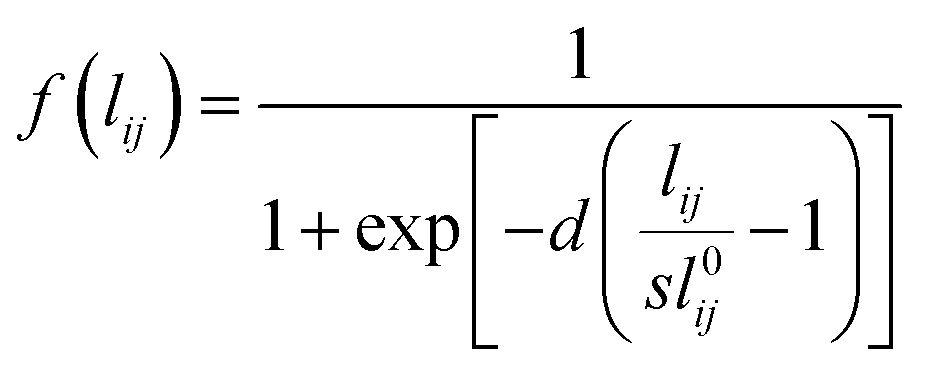
The optical properties of graphene-based nanostructures are studied by exploiting ωFQ, which is a classical, fully atomistic approach, which modulates Drude conduction with quantum tunneling effects.30–33 In particular, each atom is endowed with a complex-valued charge qi, which adjusts to the external oscillating electric field E(ω). The set of charges q is obtained by solving an equation of motion, where charge-exchange between atoms is governed by a Drude mechanism, and modulated through quantum tunneling. In the frequency domain, the classical ωFQ equation of motion for charges q in graphene-based materials reads:32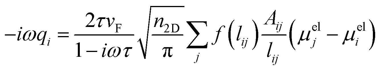 | (1) |
 | (2) |
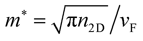 ,59 whereas the Fermi energy is defined as
 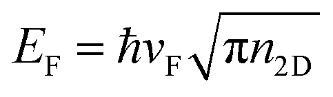 , leading to an electronic density which depends on EF, which can be tuned according to the experimentally applied gating. The external electric field induces an electric field on the nanostructure, which is calculated from the Gaussian charge distributions on each atom. Unless otherwise stated, in all calculations we set EF = 400 meV, τ = 600 a.u. (i.e. 14.5 fs) and vF = 106 m s−1τ is fitted against reference ab initio63 data in order to take into account scattering processes leading to plasmon relaxation (see Fig. 1). In particular, for plasmon energies above the phonon threshold energy (of ≈0.2 eV), the electron–phonon coupling dominates the plasmon decay and the scattering time becomes of the order of 10−14 s.64–68 Therefore, the fitted τ = 14.5 fs takes into account both decay channels.
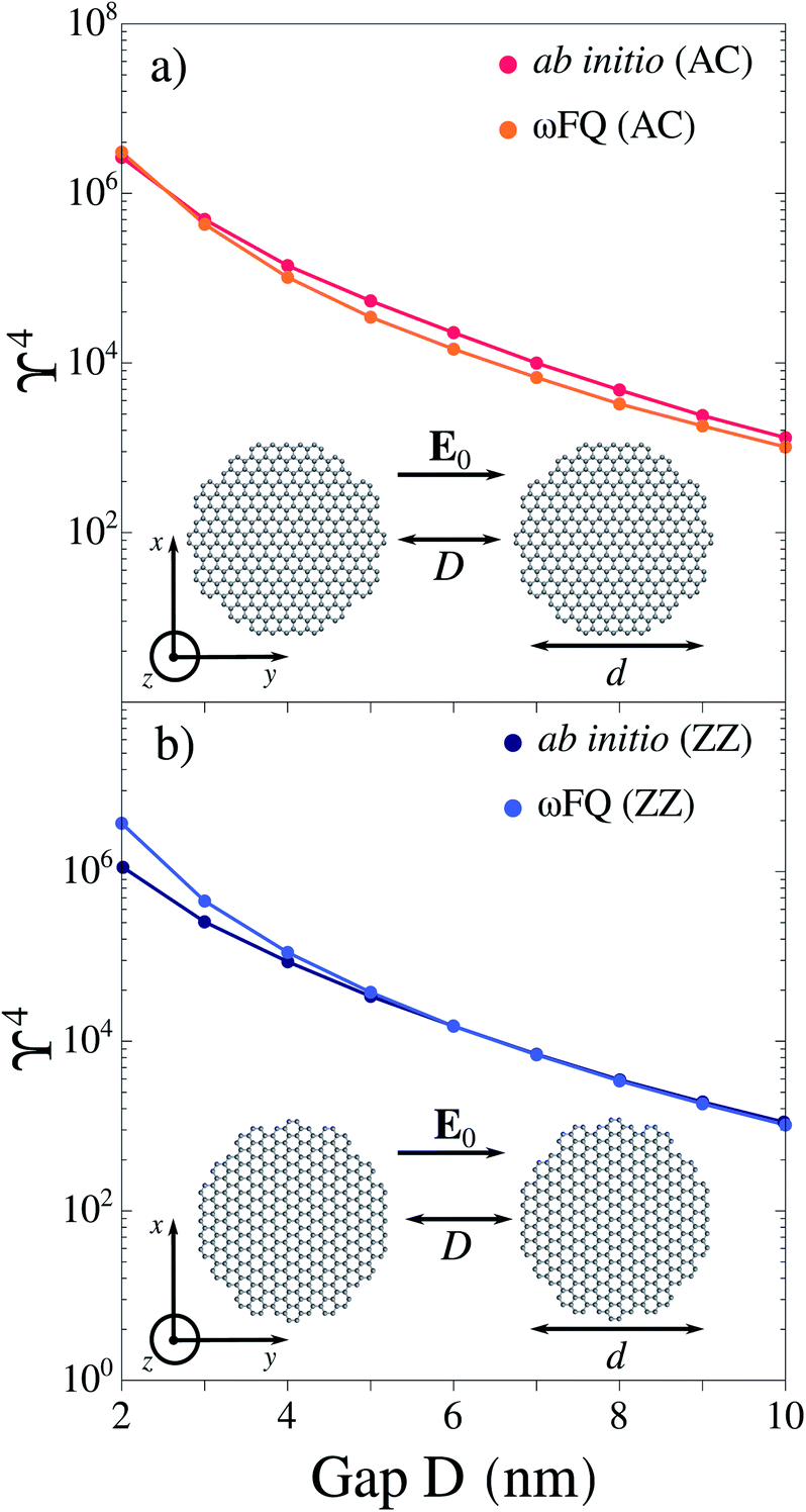 | ||
| Fig. 1 ωFQ and ab initio (reproduced from ref. 63) ϒ4 values for (a) AC–AC and (b) ZZ–ZZ graphene dimers (d = 20 nm) as a function of the gap width D. The graphene Fermi energy is EF = 0.4 eV for each configuration. | ||
3. Results and discussion
3.1 Model validation
We first study the electric field enhancement (ϒ = |E|/|E0|) exhibited by planar graphene dimeric nanoantennas (see Sec. S1 and S3 in the ESI†). In particular, we consider monomers with circular shape (with diameter d ∼ 20 nm), and dimers obtained by coupling armchair (AC) or zig-zag (ZZ) graphene monomers at a distance D (see Fig. 1a and b for their structures). In our simulations, the external electric field is polarized along the y direction (see Fig. 1a and b). We calculate the field enhancement associated with GERS process, which is proportional to ϒ4,21 at the center of mass of the whole system, in the graphene plane (i.e. z = 0 nm), at the PRF of each dimer (see also Sec. S3 in the ESI†). For both AC and ZZ configurations, the considered PRF is associated with a boundary dipolar plasmon (BDP), i.e. a dipolar plasmon arises in each monomer. In Fig. 1a and b, ωFQ results are compared with ab initio data reproduced from ref. 63; the agreement between the two methods is impressive, thus demonstrating the level of reliability of the classical ωFQ method. Only a minor discrepancy is observed for ZZ–ZZ with D = 2 nm gap. This is probably due to edge effects which cause an increase of the field confinement in the proximity of the gap and, as a consequence, a slight increase in the field enhancement. Such edge effects become negligible by increasing the gap (D ≥ 4 nm). In line with ab initio results,63 ωFQ predicts the maximum field enhancement for the smallest gap (D = 2 nm) and a rapid decrease as the width of the nanojunction increases. Additional comparison between ωFQ and ab initio results for selected circular and triangular graphene-based arrangements are reported in Sec. S3 of the ESI,† showing again almost perfect agreement. These findings confirm the reliability of ωFQ to describe the electric field enhancement in graphene-like structures.3.2 Pristine graphene sheets
We now take advantage of ωFQ favourable computational scaling,33 to study electric field enhancement in several graphene disks of increasing size (see also Sec. S4 in the ESI†), with a diameter D from 2 nm (112 atoms) to 200 nm (more than 1.1 million atoms). In Fig. 2, the electric field is computed at the center of the disk, at d = 3.5 Å from the substrate (in line with the average adsorption distance of molecules on graphene7,69,70), and at distance s = 3.5 Å from the side of the disk. Both enhancements are computed at the PRF of the dipolar plasmon mode of each disk (see inset in Fig. 2). We first focus on the enhancement computed at the center of the disk. ϒ4 decreases as the disk size increases, however, for small diameters, ϒ4 increases due to edge effects, which become negligible for D ≥ 20 nm. Remarkably, for diameters typically exploited in GERS experimental setups (i.e. D ≫ 50 nm), the enhancement is strongly reduced and tends to ϒ4 ∼ 40 for D = 200 nm. On the other hand, ϒ4 calculated at the edges is three orders of magnitude larger than the values at the center (see right axis in Fig. 2). In particular, ϒ4 increases with the dimension of the disk and converges to ϒ4 ≈ 8.0 × 10⁵ for D ≥ 120 nm. However, notice that such large ϒ4 values rapidly decay by receding from the edges, bringing no benefit to potential spectral enhancements in case of adsorbed molecular systems, which are generally placed away from edges.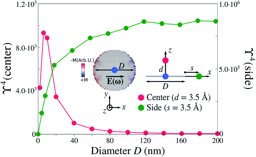 | ||
| Fig. 2 Calculated ϒ4 for pristine graphene disks as a function of the diameter D. Values are computed at the dipolar plasmon mode (see inset for a graphical representation) at two specific points: the center of the disk (blue dot) at distance d = 3.5 Å (red dot), and at a distance s = 3.5 Å from the edge (green dot). The Fermi energy is equal to EF = 0.4 eV in all calculations. | ||
3.3 Graphene tips
We focus on graphene tips based on 3D bow-tie antennas obtained by pairing two hollow carbon nanocones forming a nanocavity (see Fig. 3a). Such structures are inspired by the graphene 2D bow-tie antennas which we studied above to validate the method.63,71,72 Hollow graphene nanocones have been experimentally reported.73–76 In addition, graphene nanocones are currently exploited for the encapsulation of gold tips in atomic force microscopy (AFM) experiments to increase their mechanical stability.77 The studied geometries are constructed by removing a slice of α angle from a circular graphene sheet, and welding together the two parts, for a given height h (see Fig. 3a). By varying both α and h, the β angle defining the sharpness can easily be tuned. Here we select β = 30° and β = 40° to study the dependence of ϒ4 on the nanocone shrinking. In fact, the nanocones have a very sharp, atomistically defined, vertex, which is constituted of 3 (β = 30°) or 4 carbon atoms (β = 40°). The considered 3D bow-ties are formed by coupling two facing nanocones at distance D; electric field is always polarized along the axis connecting them.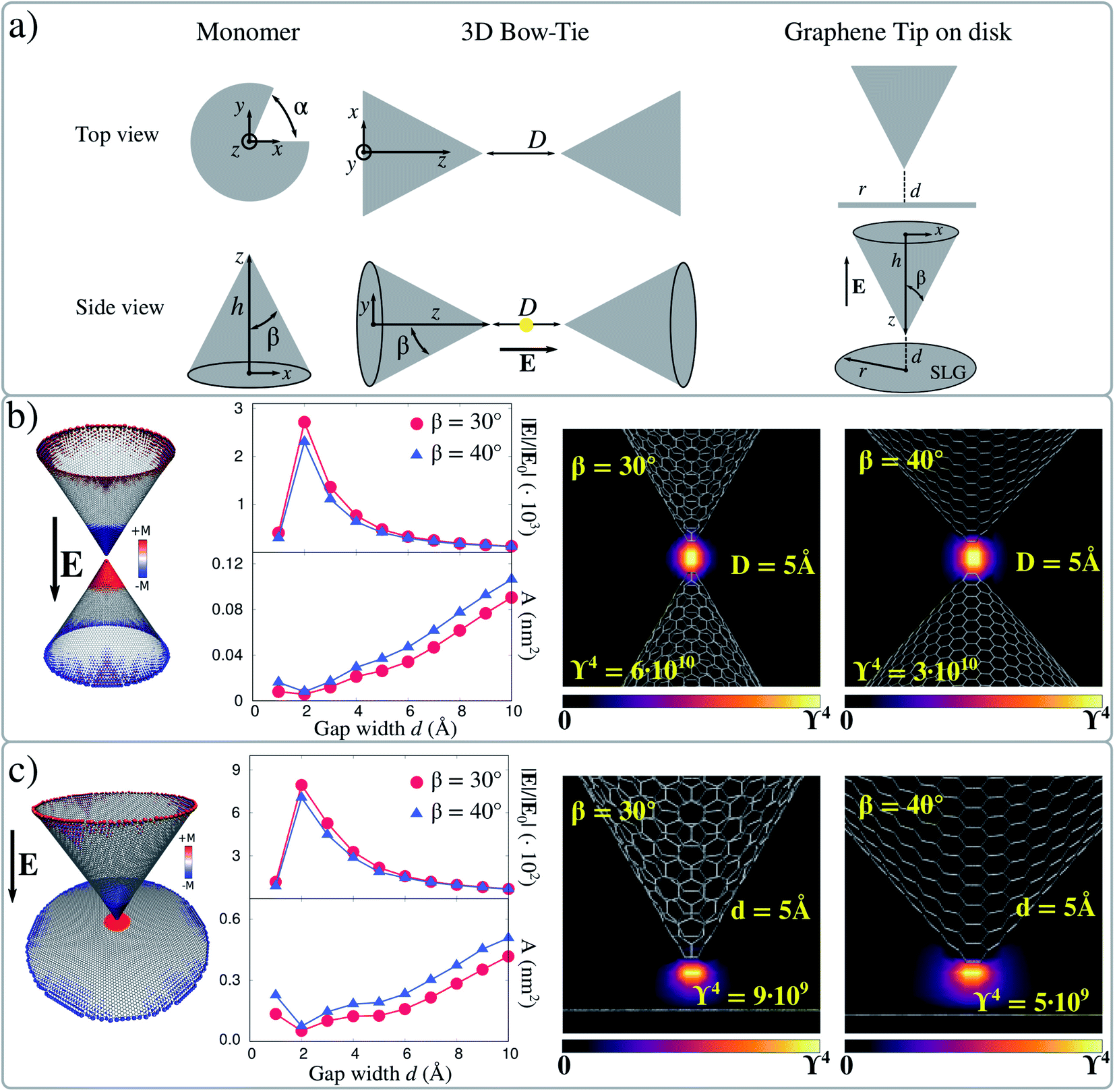 | ||
| Fig. 3 (a) Geometrical parameters of graphene-based nanocones, 3D bow-ties and graphene tip-disks. (b) 3D bow-tie electric field enhancement factors (|E|/|E0| and ϒ4) and localization area (A) for both β = 30° and β = 40°, as a function of the gap width (D) calculated at the boundary dipolar plasmon (see left panel) in the center of the gap. β = 30° and β = 40° electric field enhancement factors color map for 3D bow-tie nanostructure with D = 5 Å. (c) Graphene tip-disk electric field enhancement factors (|E|/|E0| and ϒ4) and localization area (A) for both β = 30° and β = 40°, as a function of the gap width (d) calculated at the boundary dipolar plasmon (see left panel) in the center of the gap. β = 30° and β = 40° electric field enhancement factors color maps for graphene tip-disk nanostructure with d = 5 Å. The Fermi level is set to EF = 0.4 eV for each configuration. | ||
Computed ϒ4 values for the boundary dipolar plasmon mode (see S5 in the ESI†) at the center of the gap as a function of D are reported in Fig. 3b. The maximum value of |E|/|E0| (2.0 × 10³) corresponds to D = 2 Å for both configurations, and rapidly decreases as D increases. |E|/|E0| is larger for the structures with β = 30°, due to the presence of a sharper tip, although computed fields are of the same order of magnitude. Also, |E|/|E0| is strongly reduced for D = 1 Å, however the two monomers are almost covalently bonded at this distance and thus a dramatic change in their optical properties is expected.
In order to fully characterize the field enhancement, the local character of the enhanced electric field can be quantified. Such a feature is deeply connected to the actual resolution of surface enhanced spectral signals. By following ref. 44 and 78, the effective localization area A is defined as:
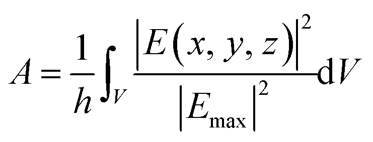 | (3) |
An alternative geometrical arrangement can be designed by coupling a tip and a sheet, where a molecular system can potentially be deposited, similarly to what is done in case of tip enhanced spectroscopies.34,38–40 Therefore, plasmonic picocavities can be created by placing a graphene sheet (in our case, a graphene disk with radius 10 nm) at close distance from the apex of a nanocone (see Fig. 3a). Also in this case, we perform the same simulations as for the 3D bow-tie system, by varying the gap between the sheet and the apex (d) from 1 to 10 Å. The electric field enhancement is calculated at the boundary dipolar plasmon resonance frequency, which is associated with a dipolar mode involving both the cone and the graphene disk (see Fig. 3c). |E|/|E0| rapidly decreases as the gap increases, while the opposite trend is observed for the effective localization area A, which is in this case computed for a slice centered in the middle of the gap. The same also holds for small gaps, for which the two structures are bonded. Finally, ϒ4 is graphically reported for both β = 30 and β = 40° and d = 5 Å, as computed in the plane parallel to the electric field direction. For both angles, ϒ4 is about 109, thus one order of magnitude lower than for 3D bow-ties. This behavior is expected, because in tip-disk structures a single tip is responsible for the huge electric field enhancement. However, this geometrical arrangement is promising and could be exploited in GERS experiments. In fact, it returns enhancement factors that, according to our calculations, could be up to seven orders of magnitude larger than those commonly reached in current GERS experiments exploiting pristine graphene as substrates. Also, it might provide huge field localization, thus allowing excellent spectral resolution. To conclude, for both 3D bow-ties and tip-disk arrangements, we focused on the dipolar plasmon where charges accumulate near the tips of both structures. Remarkably, the dipolar nature of these plasmon modes does not change by increasing the size of these systems.
3.4 Bite defects
We now move to investigate structures bearing atomic-scale defects. We first focus on AC and ZZ graphene nanoribbons. Their geometries are constructed according to the experimental structures reported in ref. 46 (see Fig. 4). In particular, the number of missing rings forming the bite defects and the relative distance between two adjacent defects resemble those experimentally measured.46 There, atomically precise fabrication methods are exploited, which in principle allow for a deep control of the system's geometry.50 However, the resulting samples may contain a certain percentage of structural disorder due to missing benzene rings resulting from the synthesis.48,49 These defects are known as bite defects and affect charge transport along the nanoribbon through charge confinement.46,47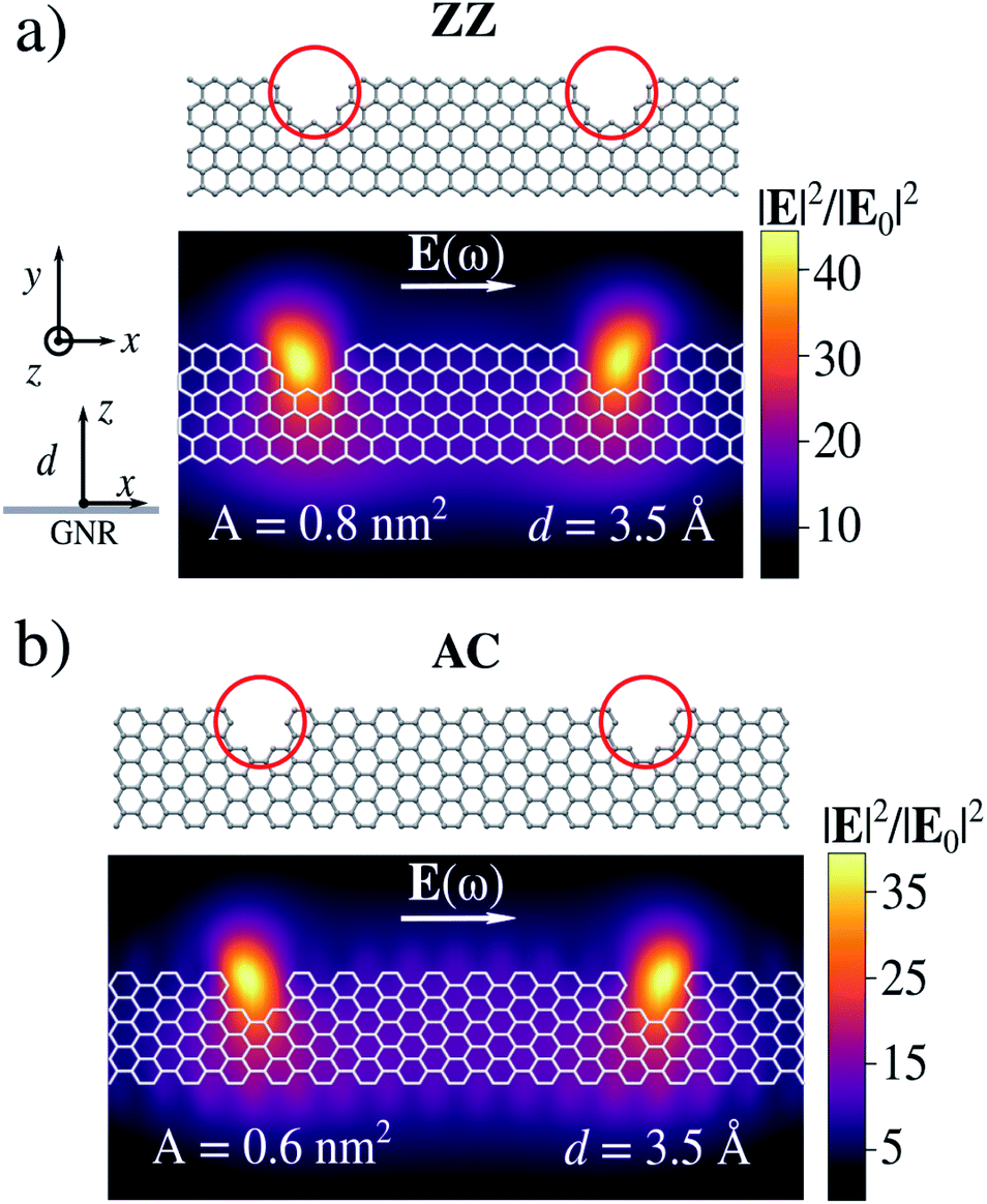 | ||
| Fig. 4 Geometries and electric field enhancement factor (|E|2/|E0|2) color maps for ZZ (a) and AC (b) graphene nanoribbons with bite defects. Color maps are calculated at distance d = 3.5 Å from the nanostructure. The Fermi energy is set equal to EF = 0.4 eV. | ||
Electric field enhancements (|E|2/|E0|2) for both AC and ZZ GNRs with bite defects are computed at their PRFs, on a plane placed at d = 3.5 Å (see Fig. 4). When the incident electric field is polarized along the x-direction, i.e. the system main axis, the plasmon excitation is associated with a localization of charge around the bite, in both AC or ZZ configurations. Such localization is associated with ϒ4 larger than 103 at d = 3.5 Å. Thus, bite defects strongly trap plasmons, leading to the formation of hot-spots. Similar to the previous cases, we can quantify the local character of the enhanced electric field by means of its effective localization area A, which is reported in Fig. 4. The induced electric field is localized inside the bite and the effective area is subnanometric. Interestingly, in this case the huge atomistic localization of the electric field follows the presence of a hole in the structure, whereas in more common nanostructures tips/needles are exploited.
From the numerical point of view, the enhancement is much lower than in the case of cone-based structures (see above). A possible strategy to increase the induced fields would consist of exploiting one of the most peculiar properties of graphene, i.e. the Fermi level tunability. In fact, by increasing the Fermi energy (EF), the number of electrons involved in the collective excitation increases, and in turn also the electric field. Thus, we vary EF from 0.2 eV to 1.0 eV (see Section S6 in the ESI†), which is a range experimentally achievable.4,79 The enhancement factors increase by increasing EF, without any loss in the induced fields local character. We finally notice that, similar to the corresponding experimental setups, the systems are composed of a relatively small number of atoms; therefore, even larger field enhancement factors are expected for bigger nanostructures.
3.5 Strained polycrystalline graphene sheets
In this section we focus on a 40 nm × 40 nm polycrystalline graphene (PCG) sheet, as shown in Fig. 5a. The interest in studying such structure is driven by two reasons. First, PCGs are experimentally accessible.51–53,80–84 Secondly, as we have already shown and discussed above, the generation of high field enhancement and confinement, i.e. hot-spots, in large graphene-based systems is particularly challenging.28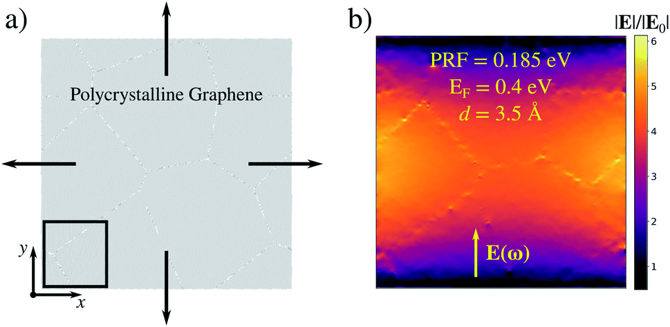 | ||
| Fig. 5 (a) Graphical representation of the stretching process of a PCG sheet of 40 nm of side. The black box highlights the region where the maximum field enhancement for the stretched structure is computed. (b) ϒ color map arising for the pristine PCG sheet at rest. The Fermi energy is set to 0.4 eV. | ||
To create regions characterized by large electric field enhancement and confinement, we apply a mechanical stress to PCG in terms of an isotropic strain. Note that dimensions comparable with those exploited in the present work (40 nm × 40 nm) have been used to model the cracking of experimentally studied graphene sheets.51,85,86 To simulate the stretching process, we perform a reactive molecular dynamics (MD) calculation employing ReaxFF87,88 on PCG, where a strain rate of  is applied along the x and y directions for 56 ps (see Fig. 5a and Sec. S2 in the ESI† for more details about the computational protocol). From the MD we extract six snapshots (see Sec. S7 in the ESI†) at different strain percentages ∈. Each geometry is then excited by an external monochromatic electric field polarized along the y direction and oscillating at the PRF of the considered geometry see Fig. 5a. For all the snapshots, the maximum field enhancement ϒ4 is computed in the region highlighted in the black box in Fig. 5a, on a plane parallel to the PCG and placed at 3.5 Å from it. This region has been chosen because it corresponds to the area where the first crack starts to form (see Sec. S7 in the ESI†).
To evaluate the effects of defects formation, we compare the field enhancement computed for each geometry with those of the structure at rest. Pristine PCG features a dipolar plasmon at 0.185 eV; the charge density is localized at the edge of the structure (not shown), similarly to what we observed previously (e.g. see Fig. 2). The field enhancement away from the edge is low, i.e. ϒ4 = 1.2 × 10³ (see Fig. 5b).
As a result of the application of a tensile stress, cracks are first formed in the substrate, then they propagate across the sample, in agreement with previous observations.51 Thus, narrow gaps between adjacent regions appear and, by further increasing the strain, the graphene sheet breaks completely (see Sec. S7 in the ESI†). As soon as defects are formed, plasmon confinement and field enhancement are observed in regions away from PCG edges (see Fig. 6a–f). A clear dependence of the enhancement upon the applied strain is not observed (see Fig. 6), whereas plasmon charges are indeed confined on edges and defects along the cracks. This suggests that once a crack starts forming, the kinetics of the cracking process is correlated to the reported enhancement more than the actual strain which is applied. However, high field enhancement and subnanometric localization are simultaneously reached in certain surface regions for different ∈ values. The highest enhancement occurs for ∈ = 4.18%, being ϒ4 = 3.9 × 10⁹ and the effective localization area A = 0.17 nm2 (see Fig. 6c). Therefore, the isotropic strain deformation of PCG seems to induce the formation of highly confined and enhanced fields, i.e. hot-spots, along the cracks. Moreover, it is known that graphene edges and vacancies can act as adsorption sites for various types of analytes.89–92 Although this is not directly proven in this work, our results suggest that morphological defects not only behave as hot-spots, but can be ideal candidates for adsorption of target analytes, in order to allow their probing through surface-enhanced spectral signals. Therefore, common shortcomings of graphene substrates in the context of surface-enhanced spectroscopies might be solved through defect engineering.
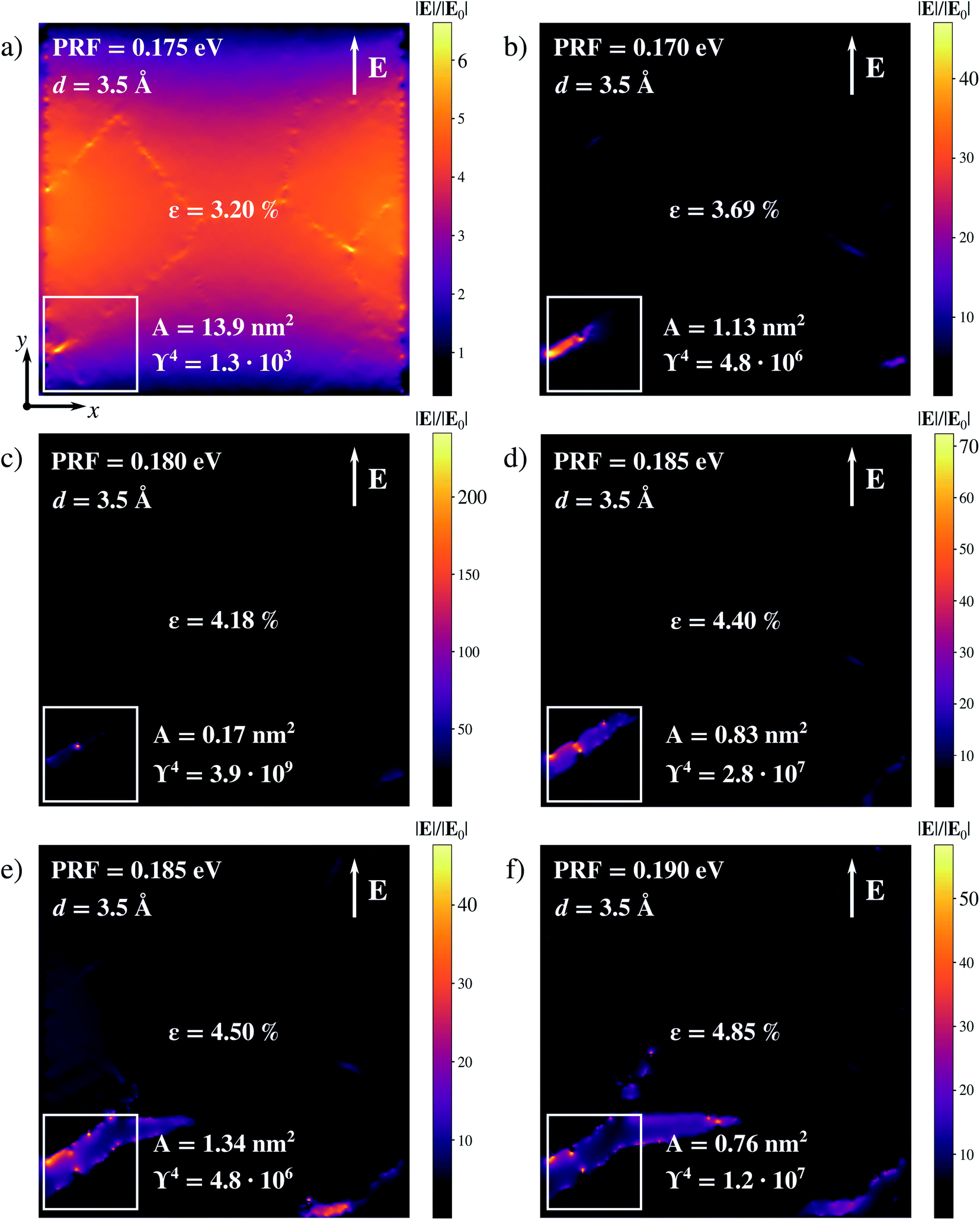 | ||
| Fig. 6 Computed |E|/|E0| color maps of PCG under isotropic strain ∈ = 3.20% (a), 3.69% (b), 4.18% (c), 4.40% (d), 4.50% (e) and 4.85% (f). The maximum enhancement is calculated in the region highlighted in the white box. The Fermi level is set to EF = 0.4 eV for all calculations. | ||
4. Summary and conclusions
We have shown that high electric field enhancement and confinements can arise in engineered graphene-based nanostructures. The latter are designed by following two approaches. The first mimics geometrical arrangements commonly exploited to create hot-spots with noble MNPs, such as 3D bow-tie antennas. The second exploits graphene peculiar properties, such as edge defects and cracks propagating in polycrystalline substrates. Computed field enhancement and confinement factors show that in all these structures hot-spots are induced, which can be used as potential substrate for surface-enhanced spectroscopies. Notably, in some cases the computed field enhancement is comparable with the values which are observed in widely-used metal nanosubstrates exploited in SERS, thus suggesting that single-molecule detection is potentially accessible also in graphene-based nanostructures. In addition, computed confinement factors go down to the subnanometric scale, thus also suggesting a huge potentiality of graphene to strongly confine plasmon-induced enhancement. To conclude, the findings of this study suggest that by proper engineering graphene-based structures, the common shortcomings reported for graphene when it is exploited as a substrate for surface-enhanced spectroscopies can be solved. We hope that our work can inspire further experimental investigations to confirm our theoretical predictions.Conflicts of interest
There are no conflicts to declare.Acknowledgements
This work has received funding from the European Research Council (ERC) under the European Union's Horizon 2020 research and innovation program (grant agreement No. 818064). We acknowledge the Center for High Performance Computing (CHPC) at SNS for providing the computational infrastructure.References
- A. Grigorenko, M. Polini and K. Novoselov, Nat. Photonics, 2012, 6, 749–758 CrossRef CAS.
- F. H. Koppens, D. E. Chang and F. J. Garcia de Abajo, Nano Lett., 2011, 11, 3370–3377 CrossRef CAS PubMed.
- Z. Fang, S. Thongrattanasiri, A. Schlather, Z. Liu, L. Ma, Y. Wang, P. M. Ajayan, P. Nordlander, N. J. Halas and F. J. García de Abajo, ACS Nano, 2013, 7, 2388–2395 CrossRef CAS PubMed.
- F. J. Garcia de Abajo, ACS Photonics, 2014, 1, 135–152 CrossRef CAS.
- A. C. Ferrari, F. Bonaccorso, V. Fal’Ko, K. S. Novoselov, S. Roche, P. Bøggild, S. Borini, F. H. Koppens, V. Palermo and N. Pugno, et al. , Nanoscale, 2015, 7, 4598–4810 RSC.
- X. Ling, S. Huang, S. Deng, N. Mao, J. Kong, M. S. Dresselhaus and J. Zhang, Acc. Chem. Res., 2015, 48, 1862–1870 CrossRef CAS PubMed.
- S. Huang, X. Ling, L. Liang, Y. Song, W. Fang, J. Zhang, J. Kong, V. Meunier and M. S. Dresselhaus, Nano Lett., 2015, 15, 2892–2901 CrossRef CAS PubMed.
- F. Schedin, E. Lidorikis, A. Lombardo, V. G. Kravets, A. K. Geim, A. N. Grigorenko, K. S. Novoselov and A. C. Ferrari, ACS Nano, 2010, 4, 5617–5626 CrossRef CAS PubMed.
- W. Xu, X. Ling, J. Xiao, M. S. Dresselhaus, J. Kong, H. Xu, Z. Liu and J. Zhang, Proc. Natl. Acad. Sci., 2012, 109, 9281–9286 CrossRef CAS PubMed.
- H. Lai, F. Xu, Y. Zhang and L. Wang, J. Mater. Chem. B, 2018, 6, 4008–4028 RSC.
- Y. Liu, X. Dong and P. Chen, Chem. Soc. Rev., 2012, 41, 2283–2307 RSC.
- X.-M. Lin, Y. Cui, Y.-H. Xu, B. Ren and Z.-Q. Tian, Anal. Bioanal. Chem., 2009, 394, 1729–1745 CrossRef CAS PubMed.
- F. J. G. de Abajo, Science, 2013, 339, 917–918 CrossRef PubMed.
- M. G. Albrecht and J. A. Creighton, J. Am. Chem. Soc., 1977, 99, 5215–5217 CrossRef CAS.
- D. L. Jeanmaire and R. P. Van Duyne, J. Electroanal. Chem. Interfacial Electrochem., 1977, 84, 1–20 CrossRef CAS.
- A. Campion and P. Kambhampati, Chem. Soc. Rev., 1998, 27, 241–250 RSC.
- K. A. Willets and R. P. Van Duyne, Annu. Rev. Phys. Chem., 2007, 58, 267–297 CrossRef CAS PubMed.
- R. Alvarez-Puebla, L. M. Liz-Marzán and F. J. García de Abajo, J. Phys. Chem. Lett., 2010, 1, 2428–2434 CrossRef CAS.
- E. Le Ru and P. Etchegoin, Principles of Surface-Enhanced Raman Spectroscopy: And Related Plasmonic Effects, Elsevier, 2008 Search PubMed.
- S. A. Maier, Plasmonics: Fundamentals and Applications, Springer Science & Business Media, 2007 Search PubMed.
- J. Langer, D. Jimenez de Aberasturi, J. Aizpurua, R. A. Alvarez-Puebla, B. Auguié, J. J. Baumberg, G. C. Bazan, S. E. Bell, A. Boisen and A. G. Brolo, et al. , ACS Nano, 2019, 14, 28–117 CrossRef PubMed.
- K. Kneipp, Y. Wang, H. Kneipp, L. T. Perelman, I. Itzkan, R. R. Dasari and M. S. Feld, Phys. Rev. Lett., 1997, 78, 1667 CrossRef CAS.
- S. Nie and S. R. Emory, Science, 1997, 275, 1102–1106 CrossRef CAS PubMed.
- H. Xu, J. Aizpurua, M. Käll and P. Apell, Phys. Rev. E: Stat. Phys., Plasmas, Fluids, Relat. Interdiscip. Top., 2000, 62, 4318 CrossRef CAS PubMed.
- A. B. Zrimsek, N. Chiang, M. Mattei, S. Zaleski, M. O. McAnally, C. T. Chapman, A.-I. Henry, G. C. Schatz and R. P. Van Duyne, Chem. Rev., 2017, 117, 7583–7613 CrossRef CAS PubMed.
- R. Zhang, Y. Zhang, Z. Dong, S. Jiang, C. Zhang, L. Chen, L. Zhang, Y. Liao, J. Aizpurua and Y. e. Luo, et al. , Nature, 2013, 498, 82–86 CrossRef CAS PubMed.
- S. Jiang, Y. Zhang, R. Zhang, C. Hu, M. Liao, Y. Luo, J. Yang, Z. Dong and J. Hou, Nat. Nanotechnol., 2015, 10, 865–869 CrossRef CAS PubMed.
- X. Ling, L. Xie, Y. Fang, H. Xu, H. Zhang, J. Kong, M. S. Dresselhaus, J. Zhang and Z. Liu, Nano Lett., 2010, 10, 553–561 CrossRef CAS PubMed.
- X. Ling, L. Moura, M. A. Pimenta and J. Zhang, J. Phys. Chem. C, 2012, 116, 25112–25118 CrossRef CAS.
- T. Giovannini, M. Rosa, S. Corni and C. Cappelli, Nanoscale, 2019, 11, 6004–6015 RSC.
- L. Bonatti, G. Gil, T. Giovannini, S. Corni and C. Cappelli, Front. Chem., 2020, 8, 340 CrossRef CAS PubMed.
- T. Giovannini, L. Bonatti, M. Polini and C. Cappelli, J. Phys. Chem. Lett., 2020, 11, 7595–7602 CrossRef CAS PubMed.
- P. Lafiosca, T. Giovannini, M. Benzi and C. Cappelli, J. Phys. Chem. C, 2021, 125, 23848–23863 CrossRef CAS PubMed.
- F. Benz, M. K. Schmidt, A. Dreismann, R. Chikkaraddy, Y. Zhang, A. Demetriadou, C. Carnegie, H. Ohadi, B. De Nijs and R. Esteban, et al. , Science, 2016, 354, 726–729 CrossRef CAS PubMed.
- S. F. Tan, Molecular Electronic Control over Tunneling Charge Transfer Plasmons Modes, Springer, 2018, pp. 51–67 Search PubMed.
- J. J. Baumberg, J. Aizpurua, M. H. Mikkelsen and D. R. Smith, Nat. Mater., 2019, 18, 668–678 CrossRef CAS PubMed.
- A. Xomalis, X. Zheng, A. Demetriadou, A. Martínez, R. Chikkaraddy and J. J. Baumberg, Nano Lett., 2021, 21, 2512–2518 CrossRef CAS PubMed.
- R. Chikkaraddy, B. De Nijs, F. Benz, S. J. Barrow, O. A. Scherman, E. Rosta, A. Demetriadou, P. Fox, O. Hess and J. J. Baumberg, Nature, 2016, 535, 127–130 CrossRef CAS PubMed.
- B. Yang, G. Chen, A. Ghafoor, Y. Zhang, Y. Zhang, Y. Zhang, Y. Luo, J. Yang, V. Sandoghdar and J. Aizpurua, et al. , Nat. Photonics, 2020, 14, 693–699 CrossRef CAS.
- P. Liu, D. V. Chulhai and L. Jensen, ACS Nano, 2017, 11, 5094–5102 CrossRef CAS PubMed.
- J. Lee, N. Tallarida, X. Chen, P. Liu, L. Jensen and V. A. Apkarian, ACS Nano, 2017, 11, 11466–11474 CrossRef CAS PubMed.
- I. Romero, J. Aizpurua, G. W. Bryant and F. J. G. De Abajo, Opt. Express, 2006, 14, 9988–9999 CrossRef PubMed.
- N. A. Hatab, C.-H. Hsueh, A. L. Gaddis, S. T. Retterer, J.-H. Li, G. Eres, Z. Zhang and B. Gu, Nano Lett., 2010, 10, 4952–4955 CrossRef CAS PubMed.
- M. Barbry, P. Koval, F. Marchesin, R. Esteban, A. G. Borisov, J. Aizpurua and D. Sánchez-Portal, Nano Lett., 2015, 15, 3410–3419 CrossRef CAS PubMed.
- E. Hao and G. C. Schatz, J. Chem. Phys., 2004, 120, 357–366 CrossRef CAS PubMed.
- M. Pizzochero, G. B. Barin, K. Cernevics, S. Wang, P. Ruffieux, R. Fasel and O. V. Yazyev, J. Phys. Chem. Lett., 2021, 12, 4692–4696 CrossRef CAS PubMed.
- M. Pizzochero, K. Čerņevičs, G. B. Barin, S. Wang, P. Ruffieux, R. Fasel and O. V. Yazyev, 2D Mater., 2021, 8, 035025 CrossRef CAS.
- S. Sun, Y. Guan, Z. Hao, Z. Ruan, H. Zhang, J. Lu, L. Gao, X. Zuo and J. Cai, Nano Res., 2021, 1–6 Search PubMed.
- P. S. Costa, J. D. Teeter, A. Enders and A. Sinitskii, Carbon, 2018, 134, 310–315 CrossRef CAS.
- J. Cai, P. Ruffieux, R. Jaafar, M. Bieri, T. Braun, S. Blankenburg, M. Muoth, A. P. Seitsonen, M. Saleh and X. Feng, et al. , Nature, 2010, 466, 470–473 CrossRef CAS PubMed.
- K. Kim, V. I. Artyukhov, W. Regan, Y. Liu, M. Crommie, B. I. Yakobson and A. Zettl, Nano Lett., 2012, 12, 293–297 CrossRef CAS PubMed.
- Z. Zhang, X. Zhang, Y. Wang, Y. Wang, Y. Zhang, C. Xu, Z. Zou, Z. Wu, Y. Xia and P. Zhao, et al. , ACS Nano, 2019, 13, 10327–10332 CrossRef CAS PubMed.
- S. R. Na, X. Wang, R. D. Piner, R. Huang, C. G. Willson and K. M. Liechti, ACS Nano, 2016, 10, 9616–9625 CrossRef CAS PubMed.
- K. J. Savage, M. M. Hawkeye, R. Esteban, A. G. Borisov, J. Aizpurua and J. J. Baumberg, Nature, 2012, 491, 574–577 CrossRef CAS PubMed.
- R. Esteban, A. G. Borisov, P. Nordlander and J. Aizpurua, Nat. Commun., 2012, 3, 1–9 Search PubMed.
- W. Zhu, R. Esteban, A. G. Borisov, J. J. Baumberg, P. Nordlander, H. J. Lezec, J. Aizpurua and K. B. Crozier, Nat. Commun., 2016, 7, 1–14 CrossRef PubMed.
- M. Urbieta, M. Barbry, Y. Zhang, P. Koval, D. Sánchez-Portal, N. Zabala and J. Aizpurua, ACS Nano, 2018, 12, 585–595 CrossRef CAS PubMed.
- X. Chen, J. E. Moore, M. Zekarias and L. Jensen, Nat. Commun., 2015, 6, 1–8 Search PubMed.
- A. C. Neto, F. Guinea, N. M. Peres, K. S. Novoselov and A. K. Geim, Rev. Mod. Phys., 2009, 81, 109 CrossRef.
- E. J. Skjølstrup, T. Søndergaard and T. G. Pedersen, Phys. Rev. B, 2018, 97, 115429 CrossRef.
- L. Stella, P. Zhang, F. García-Vidal, A. Rubio and P. García-González, J. Phys. Chem. C, 2013, 117, 8941–8949 CrossRef CAS.
- S. Raza, S. I. Bozhevolnyi, M. Wubs and N. A. Mortensen, J. Phys.: Condens. Matter, 2015, 27, 183204 CrossRef PubMed.
- S. Thongrattanasiri and F. J. G. de Abajo, Phys. Rev. Lett., 2013, 110, 187401 CrossRef PubMed.
- M. Jablan, H. Buljan and M. Soljačić, Phys. Rev. B: Condens. Matter Mater. Phys., 2009, 80, 245435 CrossRef.
- T. Low and P. Avouris, ACS Nano, 2014, 8, 1086–1101 CrossRef CAS PubMed.
- F. Karimi and I. Knezevic, Phys. Rev. B, 2017, 96, 125417 CrossRef.
- D. Novko, Nano Lett., 2017, 17, 6991–6996 CrossRef CAS PubMed.
- R. Beams, L. G. Cançado and L. Novotny, Nano Lett., 2011, 11, 1177–1181 CrossRef CAS PubMed.
- E. Voloshina, D. Mollenhauer, L. Chiappisi and B. Paulus, Chem. Phys. Lett., 2011, 510, 220–223 CrossRef CAS.
- K. Kneipp, Y. Ozaki and Z.-Q. Tian, Recent Developments In Plasmon-supported Raman Spectroscopy: 45 Years of Enhanced Raman Signals, World Scientific, 2017 Search PubMed.
- H. Liu, S. Sun, L. Wu and P. Bai, Plasmonics, 2014, 9, 845–850 CrossRef CAS.
- W. Wang, T. Christensen, A.-P. Jauho, K. S. Thygesen, M. Wubs and N. A. Mortensen, Sci. Rep., 2015, 5, 1–9 CAS.
- J. A. Jaszczak, G. W. Robinson, S. Dimovski and Y. Gogotsi, Carbon, 2003, 41, 2085–2092 CrossRef CAS.
- C.-T. Lin, C.-Y. Lee, H.-T. Chiu and T.-S. Chin, Langmuir, 2007, 23, 12806–12810 CrossRef CAS PubMed.
- S. N. Naess, A. Elgsaeter, G. Helgesen and K. D. Knudsen, Sci. Technol. Adv. Mater., 2009, 10, 065002 CrossRef PubMed.
- N. Wohner, P. Lam and K. Sattler, Carbon, 2014, 67, 721–735 CrossRef CAS.
- A. G. Cano-Marquez, W. G. Schmidt, J. Ribeiro-Soares, L. G. Cançado, W. N. Rodrigues, A. P. Santos, C. A. Furtado, P. A. Autreto, R. Paupitz and D. S. Galvão, et al. , Sci. Rep., 2015, 5, 1–5 Search PubMed.
- X. Chen and L. Jensen, Nanoscale, 2018, 10, 11410–11417 RSC.
- C.-F. Chen, C.-H. Park, B. W. Boudouris, J. Horng, B. Geng, C. Girit, A. Zettl, M. F. Crommie, R. A. Segalman and S. G. Louie, et al. , Nature, 2011, 471, 617–620 CrossRef CAS PubMed.
- O. V. Yazyev and S. G. Louie, Nat. Mater., 2010, 9, 806–809 CrossRef CAS PubMed.
- O. V. Yazyev and Y. P. Chen, Nat. Nanotechnol., 2014, 9, 755–767 CrossRef CAS PubMed.
- K. Kim, Z. Lee, W. Regan, C. Kisielowski, M. Crommie and A. Zettl, ACS Nano, 2011, 5, 2142–2146 CrossRef CAS PubMed.
- F. Banhart, J. Kotakoski and A. V. Krasheninnikov, ACS Nano, 2011, 5, 26–41 CrossRef CAS PubMed.
- P. Y. Huang, C. S. Ruiz-Vargas, A. M. Van Der Zande, W. S. Whitney, M. P. Levendorf, J. W. Kevek, S. Garg, J. S. Alden, C. J. Hustedt and Y. Zhu, et al. , Nature, 2011, 469, 389–392 CrossRef CAS PubMed.
- P. Zhang, L. Ma, F. Fan, Z. Zeng, C. Peng, P. E. Loya, Z. Liu, Y. Gong, J. Zhang and X. Zhang, et al. , Nat. Commun., 2014, 5, 1–7 CAS.
- T. Zhang, X. Li and H. Gao, Int. J. Fract., 2015, 196, 1–31 CrossRef.
- A. C. Van Duin, S. Dasgupta, F. Lorant and W. A. Goddard, J. Phys. Chem. A, 2001, 105, 9396–9409 CrossRef CAS.
- K. Chenoweth, A. C. Van Duin and W. A. Goddard, J. Phys. Chem. A, 2008, 112, 1040–1053 CrossRef CAS PubMed.
- S. N. Kim, Z. Kuang, J. M. Slocik, S. E. Jones, Y. Cui, B. L. Farmer, M. C. McAlpine and R. R. Naik, J. Am. Chem. Soc., 2011, 133, 14480–14483 CrossRef CAS PubMed.
- N. Ghaderi and M. Peressi, J. Phys. Chem. C, 2010, 114, 21625–21630 CrossRef CAS.
- L. Kong, A. Enders, T. S. Rahman and P. A. Dowben, J. Phys.: Condens. Matter, 2014, 26, 443001 CrossRef PubMed.
- Y.-H. Zhang, Y.-B. Chen, K.-G. Zhou, C.-H. Liu, J. Zeng, H.-L. Zhang and Y. Peng, Nanotechnology, 2009, 20, 185504 CrossRef PubMed.
Footnote |
| † Electronic supplementary information (ESI) available: ωFQ induced electric field. Computational details. Further validation of ωFQ model. Plasmonic properties of the systems studied in Fig. 3–5. See https://doi.org/10.1039/d2na00088a |
| This journal is © The Royal Society of Chemistry 2022 |