
Theoretical investigation of high-performance MXY (M = Mo/W, X = S/Se, and Y = Se/Te) Janus monolayers for photovoltaic and optoelectronic applications
 *a
*a
Abstract
Herein, MXY (M = Mo/W, X = S/Se, and Y = Se/Te) Janus monolayers (JMLs) are theoretically investigated to explore their numerous photovoltaic/optoelectronic (PV/OE) properties. It is predicted that the MoSSe/MoSeT/WSSe/WSeTe JMLs are semiconductors having a direct energy band gap (Eg) of 1.71/1.43/1.71/1.35 eV. In contrast, MoSTe/WSTe possesses an indirect band gap of 1.15/0.89 eV. The MoSSe/MoSeTe JMLs exhibit a red shift in the peaks of the real/imaginary part of the dielectric constant (ε1(ω))/(ε2(ω)), while the absorption coefficient (α(ω)) demonstrates a blue shift. Strikingly, the MoSeTe/WSeTe JMLs show the highest spectroscopic limited maximum efficiency (SLME) of 32.75/32.05% at a 6.28/5.72 µm thickness, which makes them highly effective for photo-absorbers. In addition, the MoSSe/WSSe JMLs also show a high SLME value of 28.15% for a critical thickness of 6.89/7.56 µm. Furthermore, the MoSeTe/WSeTe JMLs exhibit a low reverse-saturation current density, open-circuit voltage, fill-factor, and high short-circuit current, while MoSSe/WSSe exhibit high values for these parameters. In addition, MoSeTe demonstrates a large transport asymmetry, having large effective masses (m*) for holes  . In contrast, WSeTe exhibits more favorable transport properties with low m* values for electrons
  and holes
 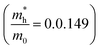 . Hence, it is our strong belief that the above-mentioned direct-band-gap JMLs with sufficiently large SLME values are the best candidates for PV and OE devices.

 Please wait while we load your content...

