Metal–semiconductor heterostructures for surface-enhanced Raman scattering: synergistic contribution of plasmons and charge transfer
Abstract
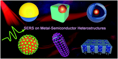
After 45 years of its first observation, surface-enhanced Raman spectroscopy (SERS) has become an ultrasensitive tool applied in chemical analysis, materials science, and biomedical research. SERS-active nanomaterials, such as noble metals, transition metals, and semiconductors, have undergone extensive development. The hybridization of semiconductors with plasmonic metal nanomaterials is highly effective in boosting light harvesting and conversion, which enables the rapid growth of metal–semiconductor hybrid nanostructures in SERS-based research fields. With the combination of the unique photoelectric properties and giant SERS signals attributed to the synergistic contribution of plasmons and change transfer (CT), metal–semiconductor heterostructures allow diverse and novel applications of SERS in CT investigations for the rational design of photovoltaic devices and ultrasensitive chemical or biological sensing. In this review, we specifically discuss SERS-active metal–semiconductor heterostructures including their building blocks, enhancement mechanisms, and applications. Moreover, we highlight the current challenges and opportunities for future research in this field based on our recent studies and other related research.


 Please wait while we load your content...