
Atomic layer deposition of high-κ layers on polycrystalline diamond for MOS devices: a review

Abstract
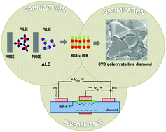
Changes in the expected performance of electronic devices have heavily influenced investigation into Si-substitute materials having the ability to meet these demands. Two examples are especially pertinent to the performance of metal oxide semiconductor (MOS) devices. The first is the move towards films with high dielectric constants (high-κ); as more components are placed onto circuit boards to facilitate the numerous system operations, the size of each device is greatly reduced necessitating exploration into more suitable options for replacing SiO2 and Al2O3 films in transistors and capacitors to effectively control semiconductor charge carriers and prevent charge leakage. The second is investigation into ultra-wide band gap (UWBG) semiconductor materials to efficiently permit device operation in harsh and extreme conditions, high temperature and high power applications. Polycrystalline diamond (PCD) is an UWBG material that provides a cost effective option for MOS devices, but it has yet to be fully studied for these applications. In addition, the combination of high-κ films on PCD for MOS components has been limited to Al2O3 despite the ability to fabricate films with higher κ values by atomic layer deposition (ALD), a technique which imparts advantages of self-limiting and saturation reactions with atomic layer control, resulting in continuous and conformal nano-thin films. It is the aim of this article therefore to highlight pertinent parameters and considerations for the optimization of high-κ materials, predominantly oxides, by ALD onto diamond film surfaces, specifically for use in MOS devices. It discusses the ALD technique and optimization of its parameters, then presents an understanding of diamond film conductivity, focussed on PCD films. Collating these two areas, it reviews high-κ film fabrication on diamond, as passivation layers and gate dielectric films. Furthermore, it examines the challenge of surface nucleation in ALD reactions and strategies for its minimization, presenting examples from literature which address this issue on 2D materials. Finally, this work culminates in a review of diamond MOS device performance as reported in literature.
- This article is part of the themed collection: Journal of Materials Chemistry C Recent Review Articles
 Please wait while we load your content...

