
Electron transfer in a semiconductor heterostructure interface through electrophoretic deposition and a linker-assisted method†
 ‡a
Xin
Tong,
ab
Daniele
Benetti,
*a
Dongling
Ma,
a
Haiguang
Zhao
*c
and
Federico
Rosei
*a
‡a
Xin
Tong,
ab
Daniele
Benetti,
*a
Dongling
Ma,
a
Haiguang
Zhao
*c
and
Federico
Rosei
*a
Abstract
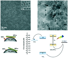
Modulating the heterostructured interface of semiconductor nanocrystals is being widely explored to enhance the charge transfer rate in photoelectrochemical cells. Here we use electrophoretic deposition and a linker-assisted method to fabricate heterostructured photoanodes based on CdSe quantum dots (QDs) or CdSe(S) nanoplates (NPLs)/TiO2 nanoparticles. The semiconductor nanocrystals exhibit red-shifted or dual photoluminescence emissions after electrophoretic deposition, due to the formation of surface traps. The calculated electron transfer rates in CdSe QDs/TiO2 nanoparticle photoanodes fabricated via electrophoretic deposition and 3-mercaptopropionic acid (MPA)-assisted attachment are 5.5 × 10⁷ s−1 and 2.7 × 10⁷ s−1, respectively, which are both higher than those obtained from NPLs/TiO2 nanoparticles ranging from 0.7 × 10⁷ s−1 to 1.3 × 10⁷ s−1. As a proof of concept, we used heterostructured semiconductor nanocrystals/TiO2 nanoparticles as photoanodes for solar-driven hydrogen generation. Upon one sun illumination, the saturated photocurrent densities of photoanodes fabricated via electrophoretic deposition were found to be higher than those of photoanodes prepared via MPA-assisted attachment, while the corresponding photoanode shows inferior long-term photostability due to the formation of surface traps on the QDs or NPLs during the electrophoretic deposition process. These results provide useful information for engineering the surface/dimension/composition of semiconductor nanocrystals, their adsorption on porous TiO2 films, and designing high-efficiency photoelectrodes in photoelectrochemical devices.
- This article is part of the themed collection: Crystal engineering for electrochemical applications
 Please wait while we load your content...

