
Solid–liquid interface optimization and properties of ultra-wide bandgap β-Ga2O3 grown by Czochralski and EFG methods
 *a
Xutang
Tao
*a
*a
Xutang
Tao
*a
Abstract
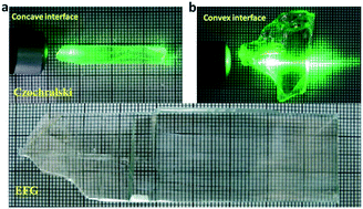
Herein, the solid–liquid interface and bulk crystal growth habit of β-Ga2O3 were studied during the Czochralski and the modified edge-defined film-fed growth (EFG) methods, respectively. The technical characteristics and process optimizations of the two methods were systematically compared and explored during the crystal growth of β-Ga2O3. In the Czochralski method, the phenomenon of spiral growth was explained based on a concave solid–liquid interface and heat transfer at high temperatures. To overcome the problem of spiral growth, a square Ir die was designed and used for the growth of β-Ga2O3 in the EFG method, and high quality β-Ga2O3 single crystals were obtained with a flat interface. The full-width at half-maximum (FWHM) of the X-ray rocking curve on the (100)-faced β-Ga2O3 grown by the EFG method was only 35.6 arcsec, indicating high crystalline quality. The carrier source of the unintentionally doped β-Ga2O3 was determined via impurity elemental analysis. A relationship between the carrier concentrations and mid-IR transmission was established. Furthermore, the PL and Raman spectra of the as-grown and annealed crystals were obtained to reveal the energy structure and stress in the crystal.
 Please wait while we load your content...

