Solution-processed metal oxide arrays using femtosecond laser ablation and annealing for thin-film transistors†
 *a
and
*a
and
Abstract
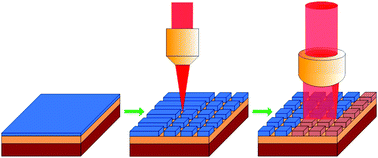
In this study, a femtosecond (fs) laser is proposed to pattern and anneal a metal oxide active layer for the facile fabrication of metal oxide thin-film transistor (TFT) arrays. Compared with conventional photolithography and lift-off techniques, fs-laser ablation significantly simplified the patterning process due to its advantages such as no contact, high yield and high resolution. Uniform patterned arrays with sharp edges and small feature size (down to 32 μm) were achieved using fs-laser ablation. Moreover, fs-laser annealing was also applied for rapid conversion of the precursor to metal oxide lattices. The results showed that an increase in laser intensity lead to an improvement in charge carrier mobility and an improvement in the on–off current ratio of indium zinc oxide (IZO) thin film transistors (TFTs) along with a negative shift of the threshold voltage. X-ray photoelectron spectroscopy (XPS) analysis indicates that an increase in laser intensity enhanced the breakdown of weak or metastable chemical bonds within IZO films, leading to the removal of hydroxide-related (OH) species and enhancement of metal oxide composition and oxygen vacancies (Ov); it facilitated carrier transport and led to an average mobility up to 9.0 cm2 V−1 s−1. Furthermore, compared with thermal annealing (TA), fs-laser annealing could reduce the thermal budget and more effectively realize the dehydroxylation behavior for OH-related species, resulting in higher charge mobility. These results clearly demonstrated that fs-laser ablation and annealing could provide a promising tool to significantly simplify the fabrication of metal oxide TFT arrays due to their advantages such as high resolution, high yield and low cost. Hence, these techniques show great potential to be applicable in the fabrication of large-area metal oxide TFT arrays for use in display devices and circuits.
- This article is part of the themed collection: 2017 Journal of Materials Chemistry C HOT Papers
 Please wait while we load your content...

