Self-screened high performance multi-layer MoS2 transistor formed by using a bottom graphene electrode†
Abstract
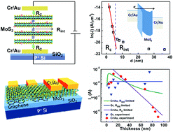
We investigated the carrier transport in multi-layer MoS2 with consideration of the contact resistance (Rc) and interlayer resistance (Rint). A bottom graphene contact was suggested to overcome the degradation of Id modulation in a back gated multi-layer MoS2 field effect transistor (FET) due to the accumulated Rint and increased Rc with increasing thickness. As a result, non-degraded drain current (Id) modulation with increasing flake thickness was achieved due to the non-cumulative Rint. Benefiting from the low Rc induced by the negligible Schottky barrier at the graphene/MoS2 interface, the intrinsic carrier transport properties immune to Rc were investigated in the multi-layer MoS2 FET. ∼2 times the enhanced carrier mobility was attained from the self-screened channel in the bottom graphene contacted device, compared to those with top metal contacts.


 Please wait while we load your content...