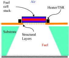
The desire for ever smarter systems-on-a-chip and plug-free portable electronics with longer operating times between recharge has stimulated growing interest in micro-ionic systems. The use of thin film and photolithographic processing techniques, commonly at temperatures considerably below those utilized in conventional ceramics processing methods, leads to ionic or mixed ionic–electronic materials with nanosized dimensions. The implications for nanosized grains on the conductivity of thin film solid oxide electrolytes are examined. Grain boundary engineering, as a means of controlling and ultimately enhancing transport along and across grain boundaries, becomes essential given that such boundaries often dominate the transport properties of such nano-dimensioned materials. Heterogeneous doping by selective in-diffusion along grain boundaries was introduced as a potentially powerful means of achieving this. This is coupled with the modeling of space charge distributions at such boundaries, taking into account possible dopant segregation to the boundaries. The use of lithographic methods for generating geometrically well defined structures is used to illustrate how one can achieve a much improved understanding of electrode processes in SOFC structures. Indeed, the more idealized structures achievable by application of microelectronic processing provide a marvelous opportunity to uncover the science underlying the technology of micro- and ultimately macro-ionics.

You have access to this article
 Please wait while we load your content...
Something went wrong. Try again?


 Please wait while we load your content...