


 PLATFORM UPDATE:


Tuning contact properties in MoSi2N4 van der Waals heterostructures with Janus metals: realizing Ohmic contacts
 *a
Jing
Pan
*a
*a
Jing
Pan
*a
Abstract
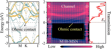
A low Schottky barrier height and high carrier tunneling probability are key figures of merit for charge transport at two-dimensional (2D) semiconductor heterojunctions. 2D MoSi2N4, with high carrier mobility and excellent stability, has emerged as a promising channel material for high-performance field-effect transistors (FETs). In this work, we investigate the contact mechanisms between 2D MoSi2N4 and MoSi2N4-derived Janus metals (MoSi2N3P1, denoted as M1; MoSi2N2P2, M2; MoSi2N2As2, M3; and MoSi2NAs3, M4) through first-principles calculations. Electronic structure analysis reveals that the M2B–MSN heterostructure (meaning that the bottom side of M2 contacts with MoSi2N4) forms a quasi-p-type Ohmic contact, while the M1B–MSN heterostructure exhibits an n-type Ohmic contact at the vertical interface with a tunneling probability, as further supported by calculations of interfacial charge transfer and redistribution. Quantum transport simulations further confirm Ohmic behavior at the M1B–MSN interface. These findings provide a theoretical basis for designing MoSi2N4-based FETs with optimized contacts.
 Please wait while we load your content...


