Crystal phase engineering of silicene by Sn-modified Ag(111)†
Abstract
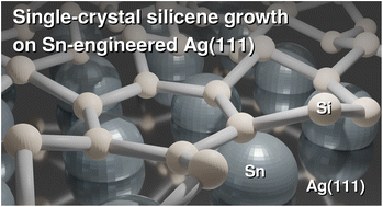
The synthesis of silicene by direct growth on silver is characterized by the formation of multiple phases and domains, posing severe constraints on the spatial charge conduction towards a technological transfer of silicene to electronic transport devices. Here we engineer the silicene/silver interface by two schemes, namely, either through decoration by Sn atoms, forming an Ag2Sn surface alloy, or by buffering the interface with a stanene layer. Whereas in both cases Raman spectra confirm the typical features as expected from silicene, by electron diffraction we observe that a very well-ordered single-phase 4 × 4 monolayer silicene is stabilized by the decorated surface, while the buffered interface exhibits a sharp  phase at all silicon coverages. Both interfaces also stabilize the ordered growth of a
  phase in the multilayer range, featuring a single rotational domain. Theoretical ab initio models are used to investigate low-buckled silicene phases (4 × 4 and a competing
  one) and various
  structures, supporting the experimental findings. This study provides new and promising technology routes to manipulate the silicene structure by controlled phase selection and single-crystal silicene growth on a wafer-scale.


 Please wait while we load your content...