Wafer-scale nanostructured black silicon with morphology engineering via advanced Sn-assisted dry etching for sensing and solar cell applications†

Abstract
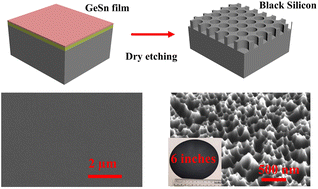
Black-Si (b-Si) providing broadband light antireflection has become a versatile substrate for photodetectors, photo-electric catalysis, sensors, and photovoltaic devices. However, the conventional fabrication methods suffer from single morphology, low yield, or frangibility. In this work, we present a high-yield CMOS-compatible technique to produce 6-inch wafer-scale b-Si with diverse random nanostructures. b-Si is achieved by O2/SF6 plasma-based reactive ion etching (RIE) of the Si wafer which is coated with a GeSn layer. A stable grid of the SnOxFy layer, formed during the initial GeSn etching, acts as a self-assembled hard mask for the formation of subwavelength Si nanostructures. b-Si wafers with diverse surface morphologies, such as the nanopore, nanocone, nanohole, nanohillock, and nanowire were achieved. Furthermore, the responsivity of the b-Si metal–semiconductor–metal (MSM) photodetector in the near-infrared (NIR) wavelength range (1000–1200 nm) is 40–200% higher than that of a planar-Si MSM photodetector with the same level of dark current, which is beneficial for applications in photon detectors, solar cells, and photocatalysis. This work not only demonstrates a new non-lithography method to fabricate wafer-scale b-Si wafers, but may also provide a novel strategy to fabricate other nanostructured surface materials (e.g., Ge or III–V based compounds) with morphology engineering.
 Please wait while we load your content...

