Inhibition of buried cavities and defects in metal halide perovskite photodetectors via a two-step spin-coating method†
Abstract
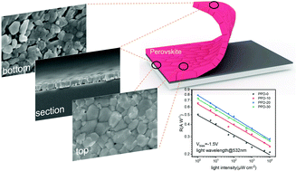
The performance of perovskite photodetectors (PPDs) is sensitive to the quality of their perovskite films. Solution-processed perovskite films suffer from excess lead halide and irregular nanocavities located at the buried interface, which result in a high dark current density and hinder the improvement of the PPD performance. Herein, we could govern the perovskite growth by introducing the modulating MAI molecule in the PbI2 precursor in a modified two-step spin-coating method. Consequently, we obtained a high-quality (large grain size, pinhole-free and well-packed) perovskite layer with uniform thickness. Also, we fabricated a photodiode-type PPD with a p–i–n configuration. At a reverse bias of −1.5 V, the optimum PPD achieved a high specific detectivity of up to 5 × 10¹¹ Jones and a decent responsivity of 0.79 A W−1 under 532 nm laser irradiation with a light intensity of 1 μW cm−2. Meanwhile, it exhibited a fast response of 2.6 μs and 72.8 μs for the rise and fall times, respectively. This strategy enriches the approaches for preparing high-quality perovskite films for diverse perovskite optoelectronic devices.


 Please wait while we load your content...