Growth of wafer-scale graphene–hexagonal boron nitride vertical heterostructures with clear interfaces for obtaining atomically thin electrical analogs†
Abstract
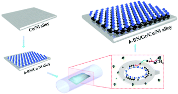
Two-dimensional (2D) integrated circuits based on graphene (Gr) heterostructures have emerged as next-generation electronic devices. However, it is still challenging to produce high-quality and large-area Gr/hexagonal boron nitride (h-BN) vertical heterostructures with clear interfaces and precise layer control. In this work, a two-step metallic alloy-assisted epitaxial growth approach has been demonstrated for producing wafer-scale vertical hexagonal boron nitride/graphene (h-BN/Gr) heterostructures with clear interfaces. The heterostructures maintain high uniformity while scaling up and thickening. The layer number of both h-BN and graphene can be independently controlled by tuning the growth process. Furthermore, conductance measurements confirm that electrical hysteresis disappears on h-BN/Gr field-effect transistors, which is attributed to the h-BN dielectric surface. Our work blazes a trail toward next-generation graphene-based analog devices.


 Please wait while we load your content...