
GaAs nanowires on Si nanopillars: towards large scale, phase-engineered arrays†

Abstract
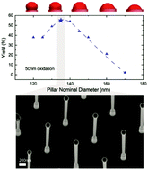
Large-scale patterning for vapor–liquid–solid growth of III–V nanowires is a challenge given the required feature size for patterning (45 to 60 nm holes). In fact, arrays are traditionally manufactured using electron-beam lithography,for which processing times increase greatly when expanding the exposure area. In order to bring nanowire arrays one step closer to the wafer-scale we take a different approach and replace patterned nanoscale holes with Si nanopillar arrays. The method is compatible with photolithography methods such as phase-shift lithography or deep ultraviolet (DUV) stepper lithography. We provide clear evidence on the advantage of using nanopillars as opposed to nanoscale holes both for the control on the growth mechanisms and for the scalability. We identify the engineering of the contact angle as the key parameter to optimize the yield. In particular, we demonstrate how nanopillar oxidation is key to stabilize the Ga catalyst droplet and engineer the contact angle. We demonstrate how the position of the triple phase line at the SiO2/Si as opposed to the SiO2/vacuum interface is central for a successful growth. We compare our experiments with simulations performed in surface evolver™ and observe a strong correlation. Large-scale arrays using phase-shift lithography result in a maximum local vertical yield of 67% and a global chip-scale yield of 40%. We believe that, through a greater control over key processing steps typically achieved in a semiconductor fab it is possible to push this yield to 90+% and open perspectives for deterministic nanowire phase engineering at the wafer-scale.
- This article is part of the themed collection: Celebrating International Women’s Day: Women in Nanoscience
 Please wait while we load your content...

