
Probing crystallographic orientation-specific carrier lifetimes in epitaxial Ge/AlAs and InGaAs/InP heterostructures
 *a
and
*a
and
Abstract
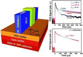
Current silicon (Si) fin transistors rely on (100) and (110) crystallographically oriented surfaces, and the proposed alternate channel transistor technology comprises materials with higher mobility than Si. Crystallographically oriented epitaxial germanium (Ge) and indium–gallium arsenide (InGaAs) have the potential to replace Si in ultra-low power transistor applications. The higher carrier lifetime is an indication of superior material quality, which relates to the leakage current of a fin transistor. To gain insights into the carrier recombination dynamics in these crystallographically oriented epitaxial Ge and InGaAs layers, the contactless microwave photoconductive decay (μ-PCD) technique at an excitation wavelength of 1500 nm was employed to probe the orientation-specific carrier lifetimes. Highly effective carrier lifetimes >200 ns for (100)Ge/AlAs and (110)Ge/AlAs, and ∼80 ns for (111)Ge/AlAs heterostructures, were extracted at room temperature. The measured carrier lifetime has a strong dependence on the surface orientation, which could be related to orientation-specific bulk trap states present within the bandgap of Ge. The (111)Ge orientation has 3 times lower carrier lifetime compared to the (100)Ge and (110)Ge surface orientations. On the other hand, the carrier lifetimes of 125 μs and 10 ns were determined from (100)InGaAs/InP and (110)InGaAs/InP heterostructures, respectively. The reduction in carrier lifetimes in both (111)Ge and (110)InGaAs was due to high electrical conductivity or higher bulk trap states present within the bandgap as well as the facet-dependent growth of the (110)InGaAs layer on InP. A surface passivating layer is indispensable for these orientation-specific epitaxial layers to improve the carrier lifetime. Therefore, the higher carrier lifetimes from technologically interesting (100)Ge and (110)Ge surfaces would offer a path for the development of Ge-based ultra-low power electronics, and optoelectronic devices based on the (100)InGaAs layer.
 Please wait while we load your content...

