GeSe photovoltaics: doping, interfacial layer and devices†

Abstract
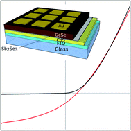
Germanium selenide (GeSe) bulk crystals, thin films and solar cells are investigated with a focus on acceptor-doping with silver (Ag) and the use of an Sb2Se3 interfacial layer. The Ag-doping of GeSe occurred by a stoichiometric melt growth technique that created Ag-doped GeSe bulk crystals. A combination of capacitance voltage measurements, synchrotron radiation photoemission spectroscopy and surface space-charge calculations indicates that Ag-doping increases the hole density from 5.2 × 1015 cm−3 to 1.9 × 1016 cm−3. The melt-grown material is used as the source for thermally evaporated GeSe films within solar cells. The cell structure with the highest efficiency of 0.260% is FTO/CdS/Sb2Se3/undoped-GeSe/Au, compared with solar cells without the Sb2Se3 interfacial layer or with the Ag-doped GeSe.
- This article is part of the themed collection: Emerging inorganic materials in thin-film photovoltaics
 Please wait while we load your content...

