Understanding the interfacial charge transfer in the CVD grown Bi2O2Se/CsPbBr3 nanocrystal heterostructure and its exploitation in superior photodetection: experiment vs. theory†

Abstract
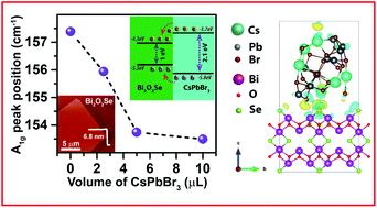
Efficient charge transfer in a 2D semiconductor heterostructure plays a crucial role in high-performance photodetectors and energy harvesting devices. Non-van der Waals 2D Bi2O2Se has enormous potential for high-performance optoelectronics, though very little is known about the interfacial charge transport at the corresponding 2D heterojunction. Herein, we report a combined experimental and theoretical investigation of interfacial charge transfer in the Bi2O2Se/CsPbBr3 heterostructure through various microscopic and spectroscopic tools corroborated with density functional theory calculations. The CVD-grown few-layer Bi2O2Se nanosheet possesses high crystallinity and a high absorption coefficient in the visible-near IR region. We integrated the few-layer Bi2O2Se nanosheet possessing superior electron mobility and CsPbBr3 nanocrystals with high light-harvesting capability for efficient broadband photodetection. The band alignment reveals a type-I heterojunction, and the device under reverse bias reveals a fast response time of 12 μs/24 μs (rise time/fall time) and an improved responsivity in the 390 to 840 nm range due to the effective interfacial charge transfer and efficient interlayer coupling at the Bi2O2Se/CsPbBr3 interface. Notably, a photodetector with a better light on/off ratio and a peak responsivity of ∼103 A W−1 was achieved in the Bi2O2Se/CsPbBr3 heterostructure due to the synergistic effects in the heterostructure under ambient conditions. The DFT analysis of the density of states and charge density plots in the heterostructure revealed a net transfer of electrons/holes from perovskite nanocrystals to Bi2O2Se layers and additional density of states in Bi2O2Se. These results are significant for the development of non-van der Waals heterostructure based high-performance low-powered photodetectors.
- This article is part of the themed collection: Nanoscale Most Popular 2021 Articles
 Please wait while we load your content...

