Quantifying thermal transport in buried semiconductor nanostructures via cross-sectional scanning thermal microscopy†
 ‡a
M. Isabel
Alonso,
c
Miquel
Garriga,
c
Benjamin J.
Robinson,
ad
Michael
Oehme,
e
Oleg V.
Kolosov
*ad
‡a
M. Isabel
Alonso,
c
Miquel
Garriga,
c
Benjamin J.
Robinson,
ad
Michael
Oehme,
e
Oleg V.
Kolosov
*ad
Abstract
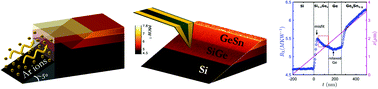
Managing thermal transport in nanostructures became a major challenge in the development of active microelectronic, optoelectronic and thermoelectric devices, stalling the famous Moore's law of clock speed increase of microprocessors for more than a decade. To find the solution to this and linked problems, one needs to quantify the ability of these nanostructures to conduct heat with adequate precision, nanoscale resolution, and, essentially, for the internal layers buried in the 3D structure of modern semiconductor devices. Existing thermoreflectance measurements and “hot wire” 3ω methods cannot be effectively used at lateral dimensions of a layer below a micrometre; moreover, they are sensitive mainly to the surface layers of a relatively high thickness of above 100 nm. Scanning thermal microscopy (SThM), while providing the required lateral resolution, provides mainly qualitative data of the layer conductance due to undefined tip–surface and interlayer contact resistances. In this study, we used cross-sectional SThM (xSThM), a new method combining scanning probe microscopy compatible Ar-ion beam exit nano-cross-sectioning (BEXP) and SThM, to quantify thermal conductance in complex multilayer nanostructures and to measure local thermal conductivity of oxide and semiconductor materials, such as SiO2, SiGex and GeSny. By using the new method that provides 10 nm thickness and few tens of nm lateral resolution, we pinpoint crystalline defects in SiGe/GeSn optoelectronic materials by measuring nanoscale thermal transport and quantifying thermal conductivity and interfacial thermal resistance in thin spin-on materials used in extreme ultraviolet lithography (eUV) fabrication processing. The new capability of xSThM demonstrated here for the first time is poised to provide vital insights into thermal transport in advanced nanoscale materials and devices.
 Please wait while we load your content...

