
Space-charge accumulation and band bending at conductive P3HT/PDIF-CN2 interfaces investigated by scanning-Kelvin probe microscopy†

Abstract
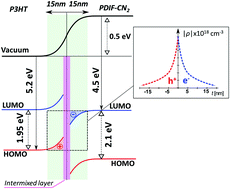
Charge transfer processes and space charge accumulation phenomena are fundamental topics concerning the technological applications of organic heterointerfaces. The possibility to achieve localized regions with enhanced charge density is, indeed, a powerful strategy to improve the performances of a vast plethora of electronic devices such as light emitting diodes, photodetectors and field-effect transistors. However, because of the complex structures of many organic compounds and the diversity of electronic interactions ruled by specific morphological features, the interfacial energy landscape of any combination of materials needs to be carefully investigated. In this work, we provide a detailed analysis of the surface potential landscape of P3HT/PDIF-CN2 donor/acceptor organic heterointerfaces. The electrical characterization, relying on the field-effect transistor configuration, outlined that the presence of a PDIF-CN2 overlayer induces a semiconductor-to-conductor transition in spin-coated P3HT OFETs. The mutual doping of the two organic materials was analyzed by Scanning Kelvin Probe Force Microscopy (SKPFM) as a function of the PDIF-CN2 coverage and nominal thickness, with the results clearly pointing at the occurrence of charge transfer phenomena between the two materials. The related band bending at the interface leads to the formation of a hole rich area within the P3HT layer and an electron rich area within the PDIF-CN2 layer. The related thickness and charge density have been estimated as 15 nm and ≈1018 cm−3, respectively. Significantly, by tuning the PDIF-CN2 overlayer coverage, the P3HT work function can be tuned within 1 eV, opening an interesting perspective for the achievement of organic optoelectronic devices with improved functionalities.
 Please wait while we load your content...

