Hysteresis-reversible MoS2 transistor
Abstract
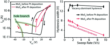
An improved understanding of the origin of the electrical transport mechanism is significant to the rational design of a high-performance electronic device. However, the complex interfacial environment and intrinsic defects in atomic-thick two-dimensional MoS2 make the electrical transport mechanism unclear. Herein, chemical vapor deposition (CVD)-grown monolayer MoS2 transistors are fabricated. The obtained results show that the hysteresis of the as-prepared MoS2 transistor is abnormal, exhibiting a different hysteresis dynamic behavior compared with that of the interfacial-trap-state-dominant hysteresis. On the basis of the temperature-resolved electrical measurement as well as Raman and photoluminescence spectroscopies, it is proposed that the abnormal hysteresis behavior is caused by the intrinsic sulfur vacancy, which leads to charge redistribution. After in situ decoration with Pt, the hysteresis behavior changes from intrinsic sulfur vacancy dominant to interfacial trap dominant due to the passivation effect, showing a hysteresis-reversible characteristic. The hysteresis width decreases from 22.30 V to 9.12 V, corresponding to the fact that the trap-state density decreases by 0.95 × 1012 cm−2. This comprehensive study not only sheds light on the mechanism underlying the electrical transport mechanism, but also offers a strategy to achieve high electrical performance.


 Please wait while we load your content...