
Atom vacancies and electronic transmission Stark effects in boron nanoflake junctions†

Abstract
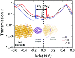
Finite-sized boron nanomaterials have received little attention in comparison to their graphene-like 2D boron analogues. It is with systems of precise atomic structures where the electrical conductance can be most fruitfully analyzed at the fundamental level. To understand how conductance varies with respect to the electronic structure, and particularly with vacancies, we study finite-sized boron nanoflakes (BNFs) and closely examine their remarkable changes in physical properties. Unlike carbon-based materials, we find from non-equilibrium Green's functions density functional theory (NEGF-DFT) calculations that the charge transport of BNFs with 35–37 atoms is modulated by site-specific atomic vacancies. The BNF with no vacancy (B37) shows significantly lower conductivity (9.23 μS), than B36 with one vacancy (46.1 μS), and lower still than with two vacancies (B35, 54.2 μS). From the thermopower function, these nanomaterials change from strong hole conductors to electron and back to hole conductors with the addition of each vacancy, from a doublet (B37) to singlet (B36) to doublet (B35) ground state, respectively. The projected density of states also reveals a trend from semiconducting to metallic-like character. A key finding is the observation of vacancy-dependent electronic transmission Stark effects (ETSEs) with respect to bias voltage (±1 V) in these molecular junctions. B37 exhibits quadratic behavior of resonance shifting, B36 shows competition between quadratic and cubic, and B35 exhibits a linear Stark effect, although this masks the nature of a cubic response at bias exceeding ±0.8 V. We prove that the vacancy position is a determining factor in the quadratic or linear ETSE behavior, from isomeric structures of these BNFs. The I–V responses also reveal that charge transport increases with vacancy for these nanoflakes. Thus, not only do vacancies affect nanoflake conductivity, but they also affect the nature of electrical transmission in the presence of a voltage bias, which is important for transistor switching. It follows then, that rather than seeking to fabricate electronic devices with pristine, defect-free boron nanoflakes, we should, however, be introducing site-specific atomic defects for high-performance devices.
- This article is part of the themed collection: Celebrating Tobin Marks’ 75th Birthday
 Please wait while we load your content...

