Vacancy engineering of a solution processed CuI semiconductor: tuning the electrical properties of inorganic P-channel thin-film transistors†

Abstract
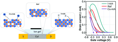
Recently, copper iodide (CuI) has been considered as a promising inorganic p-type semiconductor material. Although significant progress using CuI has been made in materials and device applications for solar cells and thin-film transistors (TFTs), little consideration has been given to the vacancy formation mechanisms and their effect on the device performance. In this work, high performance electrolyte-gated TFTs were fabricated using CuI semiconductors with different vacancy states and the origin of the threshold voltage (Vth) shift of devices in terms of vacancy species and concentration were studied. The CuI films were fabricated via a simple solution process followed by thermal annealing at low temperature (55 °C). The vacancy species and concentration in the CuI semiconductor were regulated by changing the annealing conditions as well as by introducing a dopant material. Photoluminescence (PL) and X-ray photoelectron spectroscopy (XPS) analysis were conducted to demonstrate the correlation between the electrical properties of TFTs and the vacancy states in the CuI specimens. The CuI-TFTs exhibited typical enhancement mode operation of the p-channel transistor, with sub-1 V operation voltage, ON/OFF ratio of ∼103, and high hole mobility in the range of 10–60 cm2 V−1 s−1. Experimental results revealed that Cu vacancy (VCu) play the role of inducing hole carriers, hence, TFT with VCu-rich CuI exhibited increased carrier concentration and positively shifted Vth of 0.14 V. However, iodine vacancy (VI) in CuI captures hole carriers, decreasing the concentration of charge carriers (holes), resulting to a negative Vth of −0.19 V. The TFT mobility was also affected by the vacancy concentration, owing to the carrier scattering effect. For instance, the I-rich (or VCu-rich) CuI exhibited decreased TFT mobility (14.70 cm2 V−1 s−1) due to the high carrier concentration (1019 cm−3) and their scattering effect.
 Please wait while we load your content...

