
Solution processed vertical p-channel thin film transistors using copper(i) thiocyanate†
 *d
and
Kihyon
Hong
*a
*d
and
Kihyon
Hong
*a
Abstract
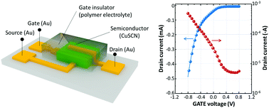
Here, we present a strategy for the realization of p-channel inorganic thin film transistors (TFTs) based on vertically stacked contacts and a copper(I) thiocyanate (CuSCN) semiconductor. The CuSCN semiconductor was generated by a simple low-temperature (ca. 100 °C) solution-based process. Utilizing the vertical architecture, channel length was determined by the thickness of the CuSCN film. This readily endows transistors with ultrashort channel lengths (<700 nm) to afford delivering drain current greatly exceeding that of conventional planar TFTs. Thus, high normalized transconductance of 0.84 S m−1 and current density of 248 mA cm−2 can be achieved for CuSCN-based vertical TFTs. To further improve the device's performance, we doped SnCl2 into the semiconductor film. By doping SnCl2 into CuSCN, shallow acceptor states that could induce additional holes were generated above the valence band maximum. The SnCl2-doped TFTs showed enlarged transconductance and current density values of 1.8 S m−1 and 541 mA cm−2, respectively, which are comparable with those of other high performance vertical transistors. The p-channel inorganic TFTs developed in this study can open up exciting opportunities in complementary circuits, display switching, and flexible electronics.
 Please wait while we load your content...

