High-mobility nanometer-thick crystalline In–Sm–O thin-film transistors via aqueous solution processing†
Abstract
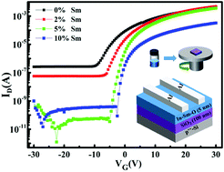
Thin-film transistors (TFTs) based on solution-derived metal oxides hold great potential in emerging low-cost large-area printed electronics. Despite recent impressive progress, these device performances are far behind those of their corresponding vacuum-based counterparts, impeding their future commercialization. In this work, we designed and created high-performance TFTs based on a nanometer-thick (down to 5 nm) crystalline In–Sm–O channel via aqueous solution processing, with a performance comparable to those of existing vacuum-processed metal oxides. The microstructural, chemical, optical, and electrical properties of the ultra-thin In–Sm–O samples as a function of Sm doping content (0–10%) were comprehensively investigated. The In–Sm–O TFTs (5% Sm) on SiO2/Si dielectrics demonstrated state-of-the-art performance, including a high mobility of 21.51 ± 1.33 cm2 V−1 s−1, subthreshold swing of 0.66 ± 0.06 V per decade, threshold voltage of 2.14 ± 0.44 V, on/off current ratio >108, and remarkable bias stress stability. The success of In–Sm–O was attributed to the high quality of the crystalline In2O3 matrix, the ideal nature of Sm dopant in suppressing oxygen vacancies, as well as the ultrathin and atomically smooth nature of the channel layer. Therefore, the aqueous solution-processed ultra-thin In–Sm–O channel is expected to enable the realization of future low-cost, large-area, and high-performance green electronics.


 Please wait while we load your content...