Atomic scale study of black phosphorus degradation†
Abstract
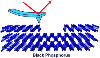
Black phosphorus (BP) is a promising two-dimensional (2D) material for future electronic devices due to its unique properties of high carrier mobility and large band gap tunability. However, thinner crystalline BP is more readily degraded under ambient conditions. For BP-based electronic devices, degradation of the exfoliated BP is a key issue. However, the nanometer scale study of BP degradation is rare so far. Herein, we report an atomically resolved degradation process of the BP surface using atomic force microscopy under temperature- and humidity-controlled environments. The atomically resolved crystal surface of BP deteriorated due to surface etching after cleavage, and showed monolayer etching. The etching process is accelerated by applying a bias voltage to BP via a conductive tip. After the voltage-assisted BP etching, the BP etching product shows crystalline BP confirmed by Raman spectroscopy and atomic force microscopy. Our atomic scale study of BP will be useful for the future 2D-based electronic devices to overcome conventional silicon-based electronic devices.


 Please wait while we load your content...