
Interfacial hybridization of Janus MoSSe and BX (X = P, As) monolayers for ultrathin excitonic solar cells, nanopiezotronics and low-power memory devices†
 a
and
Abir
De Sarkar
*a
a
and
Abir
De Sarkar
*a
Abstract
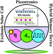
In this work, we explored the interfacial two-dimensional (2D) physics and significant advancements in the application prospects of MoSSe monolayer when it is combined with a boron pnictide (BP, BAs) monolayer in a van der Waals heterostructure (vdWH) setup. The constructed vdWHs were found to be mechanically and dynamically stable, and they form type-II p–n heterojunctions. Thus, the photogenerated electron–hole pairs are spatially separated. In the BX/MoSSe vdWHs, the BX monolayer serves as excellent donor material for MoSSe, having an ideal donor band gap of ∼1.3 eV. The small value of the conduction band offset (CBO) between the individual monolayers in the vdWHs makes it an excellent candidate for solar energy harvesting in excitonic solar cells, where the power conversion efficiencies were calculated to be 22.97% (BP/MoSSe) and 20.86% (BAs/MoSSe). Also, more than four-fold enhancement in the out-of-plane piezoelectric coefficient (d33) was observed in the MoSSe-based vdWH relative to that in the MoS2-based vdWH owing to the intrinsic built-in vertical electric field in MoSSe. This is consistent with the out-of-plane piezoelectricity brought about by the alteration in symmetry at the metal–semiconductor Schottky junction, which has been observed experimentally [M.-M. Yang, Z.-D. Luo, Z. Mi, J. Zhao, S. P. E and M. Alexe, Nature, 2020, 584, 377–381]. The results obtained in this work provide useful insights into the design of nanomaterials for future applications in nano-optoelectronics, more efficient excitonic solar cells, and nanoelectromechanical systems (NEMS). Furthermore, this work demonstrates outstanding potential for the application of these vdWHs in superfast electronics, including low-power digital data storage and memory devices, where the tunnel current between the source and drain is effectively tunable using a normal electric field of small magnitude serving as the gate voltage.
 Please wait while we load your content...

