High-mobility In and Ga co-doped ZnO nanowires for high-performance transistors and ultraviolet photodetectors†
Abstract
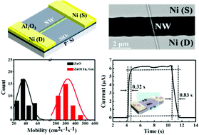
Due to their unique properties, ZnO nanostructures have received considerable attention for application in electronics and optoelectronics; however, intrinsic ZnO nanomaterials usually suffer from large concentrations of lattice defects, such as oxygen vacancies, which restricts their material performance. Here, for the first time, highly-crystalline In and Ga co-doped ZnO nanowires (NWs) are achieved by ambient-pressure chemical vapor deposition. In contrast to conventional elemental doping, this In and Ga co-doping can not only enhance the carrier concentration, but also suppresses the formation of oxygen vacancies within the host lattice of ZnO NWs. Importantly, this co-doping is also believed to effectively minimize the generation of lattice strain defects due to the optimal ionic sizes of both In and Ga dopants. When configured into field-effect transistors (FETs), these co-doped NWs exhibit an enhanced average electron mobility of 315 cm2 V−1 s−1 and an impressive on/off current ratio of 1.87 × 10⁸, which are already higher than those of other previously reported ZnO NW devices. In addition, these NW devices demonstrate efficient ultraviolet photodetection at under 261 nm irradiation with an improved responsivity of 1.41 × 10⁷ A W−1, an excellent EQE of up to 6.72 × 10⁹ and a fast response time down to 0.32 s. Highly-ordered NW parallel array thin-film transistors and photodetectors are also constructed to demonstrate the promising potential of the NWs for high-performance device applications.


 Please wait while we load your content...