Issue 5, 2020

A layered Ge2Sb2Te5 phase change material

Abstract

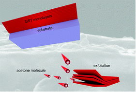
In this study, a universal Ge2Sb2Te5 phase change material was sputtered to obtain a layered structure. The crystalline phase of this material was prepared by annealing. SEM (scanning electron microscopy) and HRTEM (high-resolution transmission electron microscopy) images give confirmed that the sputtered Ge2Sb2Te5 thin film in crystalline phase has multiple layers. The layers can be exfoliated by acetone. The thicknesses of acetone-exfoliated crystalline and amorphous flakes are approx. 10–60 nm.

Graphical abstract: A layered Ge2Sb2Te5 phase change material

Supplementary files

Article information

Article type
Paper
Submitted
11 Oct 2019
Accepted
06 Jan 2020
First published
07 Jan 2020

Nanoscale, 2020,12, 3351-3358

A layered Ge2Sb2Te5 phase change material

B. Zhang, V. Cicmancova, J. Kupcik, S. Slang, J. Rodriguez Pereira, R. Svoboda, P. Kutalek and T. Wagner, Nanoscale, 2020, 12, 3351 DOI: 10.1039/C9NR08745A

To request permission to reproduce material from this article, please go to the Copyright Clearance Center request page.

If you are an author contributing to an RSC publication, you do not need to request permission provided correct acknowledgement is given.

If you are the author of this article, you do not need to request permission to reproduce figures and diagrams provided correct acknowledgement is given. If you want to reproduce the whole article in a third-party publication (excluding your thesis/dissertation for which permission is not required) please go to the Copyright Clearance Center request page.

Read more about how to correctly acknowledge RSC content.

Social activity

Spotlight

Advertisements