Electronic and optical properties of a Janus SnSSe monolayer: effects of strain and electric field
Abstract
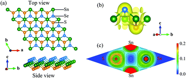
In this paper, detailed investigations of the electronic and optical properties of a Janus SnSSe monolayer under a biaxial strain and electric field using ab initio methods are presented. Our calculations indicate that the Janus SnSSe monolayer is a semiconductor with an indirect band gap larger/lower than that of the SnSe2/SnS2 monolayer. To obtain accurate estimates of the band gap, both Perdew–Burke–Ernzerhof (PBE) and Heyd–Scuseria–Ernzerhof (HSE06) hybrid functionals have been used and the effect of spin–orbit coupling has also been included. While the influence of the electric field on the electronic and optical properties of the Janus SnSSe monolayer is quite weak, biaxial strain plays a key role in controlling these properties. The Janus SnSSe monolayer has a wide absorption spectrum, from visible light to the ultraviolet region. At equilibrium, the maximum absorption coefficient of the monolayer is up to 11.152 × 104 cm−1 in the ultraviolet region and it can be increased by strain engineering. With high absorption intensity in the visible light area and being able to tune the absorbance by strain, the Janus SnSSe monolayer becomes a promising material for applications in optoelectronic devices.


 Please wait while we load your content...