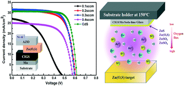
Relationship between the intermediate phases of the sputtered Zn(O,S) buffer layer and the conduction band offset in Cd-free Cu(In,Ga)Se2 solar cells†
Abstract
The Zn(O,S) layer which is alternative to the conventional CdS buffer layer is an ideal candidate due to its eco-friendly compositions and tunable bandgap. One of the approaches to further optimize the device performance is to investigate the relationship between the impurities and the conduction band offset (CBO) at the heterojunction. The impurity phases in Zn(O,S) with different oxygen fluxes are therefore analyzed and the corresponding Cd-free CIGS solar cells are investigated. We demonstrate that the value of CBO at the interface dominates the device performance in the case of low oxygen fluxes with a few impurities in the buffer layer. On the contrary, the formation of excessive impurities in the Zn(O,S) thin films prepared with high oxygen fluxes leads to the decline of the conversion efficiency of solar cells, even if the current CBO value is appropriate. Consequently, the optimized Cd-free solar cells show a similar photovoltaic performance to traditional CdS/CIGS solar cells. This result may be beneficial for preparation of high quality buffer layers and deeper understanding of the deposition of high efficiency Cd-free chalcopyrite solar cells.


 Please wait while we load your content...