Epitaxial GaN using Ga(NMe2)3 and NH3 plasma by atomic layer deposition†

Abstract
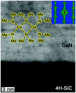
Low temperature deposition of high-quality epitaxial GaN is crucial for its integration in electronic applications. Chemical vapor deposition at approximately 800 °C using SiC with an AlN buffer layer or nitridized sapphire as substrate is used to facilitate the GaN growth. Here, we present a low temperature atomic layer deposition (ALD) process using tris(dimethylamido)gallium(III) with NH3 plasma. The ALD process shows self-limiting behaviour between 130–250 °C with a growth rate of 1.4 Å per cycle. The GaN films produced were crystalline on Si (100) at all deposition temperatures with a near stochiometric Ga/N ratio with low carbon and oxygen impurities. When GaN was deposited on 4H-SiC, the films grew epitaxially without the need for an AlN buffer layer, which has never been reported before. The bandgap of the GaN films was measured to be ∼3.42 eV and the Fermi level showed that the GaN was unintentionally n-type doped. This study shows the potential of ALD for GaN-based electronic devices.
 Please wait while we load your content...

