Tunneling-current-induced local excitonic luminescence in p-doped WSe2 monolayers†
Abstract
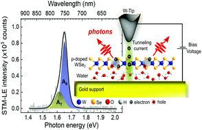
We have studied the excitonic properties of exfoliated tungsten diselenide (WSe2) monolayers transferred to gold substrates using the tunneling current in a Scanning Tunneling Microscope (STM) operated in air to excite the light emission locally. In obtained spectra, emission energies are independent of the applied bias voltage and resemble photoluminescence (PL) results, indicating that, in both cases, the light emission is due to neutral and charged exciton recombination. Interestingly, the electron injection rate, that is, the tunneling current, can be used to control the ratio of charged to neutral exciton emission. The obtained quantum yield in the transition metal dichalcogenide (TMD) is ∼5 × 10⁻⁷ photons per electron. The proposed excitation mechanism is the direct injection of carriers into the conduction band. The monolayer WSe2 presents bright and dark defects spotted by STM images performed under UHV. STS confirms the sample as p-doped, possibly as a net result of the observed defects. The presence of an interfacial water layer decouples the monolayer from the gold support and allows excitonic emission from the WSe2 monolayer. The creation of a water layer is an inherent feature of the sample transferring process due to the ubiquitous air moisture. Consequently, vacuum thermal annealing, which removes the water layer, quenches excitonic luminescence from the TMD. The tunneling current can locally displace water molecules leading to excitonic emission quenching and to plasmonic emission due to the gold substrate. The present findings extend the use and the understanding of STM induced light emission (STM-LE) on semiconducting TMDs to probe exciton emission and dynamics with high spatial resolution.


 Please wait while we load your content...