
Strain mapping inside an individual processed vertical nanowire transistor using scanning X-ray nanodiffraction†
 *a
Johannes
Svensson,
b
Abinaya
Krishnaraja,
b
Zhongyunshen
Zhu,
b
Yi
Liu,
a
Alexander
Björling,
c
Filip
Lenrick,
a
Susanna
Hammarberg,
a
Jesper
Wallentin,
a
Rainer
Timm,
a
Lars-Erik
Wernersson
b
and
*a
Johannes
Svensson,
b
Abinaya
Krishnaraja,
b
Zhongyunshen
Zhu,
b
Yi
Liu,
a
Alexander
Björling,
c
Filip
Lenrick,
a
Susanna
Hammarberg,
a
Jesper
Wallentin,
a
Rainer
Timm,
a
Lars-Erik
Wernersson
b
and
Abstract
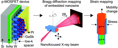
Semiconductor nanowires in wrapped, gate-all-around transistor geometry are highly favorable for future electronics. The advanced nanodevice processing results in strain due to the deposited dielectric and metal layers surrounding the nanowires, significantly affecting their performance. Therefore, non-destructive nanoscale characterization of complete devices is of utmost importance due to the small feature sizes and three-dimensional buried structure. Direct strain mapping inside heterostructured GaSb–InAs nanowire tunnel field-effect transistor embedded in dielectric HfO2, W metal gate layers, and an organic spacer is performed using fast scanning X-ray nanodiffraction. The effect of 10 nm W gate on a single embedded nanowire with segment diameters down to 40 nm is retrieved. The tensile strain values reach 0.26% in the p-type GaSb segment of the transistor. Supported by the finite element method simulation, we establish a connection between the Ar pressure used during the W layer deposition and the nanowire strain state. Thus, we can benchmark our models for further improvements in device engineering. Our study indicates, how the significant increase in X-ray brightness at 4th generation synchrotron, makes high-throughput measurements on realistic nanoelectronic devices viable.
 Please wait while we load your content...

