Revisiting thin silicon for photovoltaics: a technoeconomic perspective†
 *a
Sarah
Wieghold,
§a
*a
Sarah
Wieghold,
§a
Abstract
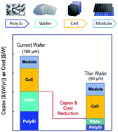
Crystalline silicon comprises 90% of the global photovoltaics (PV) market and has sustained a nearly 30% cumulative annual growth rate, yet comprises less than 2% of electricity capacity. To sustain this growth trajectory, continued cost and capital expenditure (capex) reductions are needed. Thinning the silicon wafer well below the industry-standard 160 μm, in principle reduces both manufacturing cost and capex, and accelerates economically-sustainable expansion of PV manufacturing. In this analysis piece, we explore two questions surrounding adoption of thin silicon wafers: (a) What are the market benefits of thin wafers? (b) What are the technological challenges to adopt thin wafers? In this analysis, we re-evaluate the benefits and challenges of thin Si for current and future PV modules using a comprehensive technoeconomic framework that couples device simulation, bottom-up cost modeling, and a sustainable cash-flow growth model. When adopting an advanced technology concept that features sufficiently good surface passivation, the comparable efficiencies are achievable for both 50 μm wafers and 160 μm ones. We then quantify the economic benefits for thin Si wafers in terms of poly-Si-to-module manufacturing capex, module cost, and levelized cost of electricity (LCOE) for utility PV systems. Particularly, LCOE favors thinner wafers for all investigated device architectures, and can potentially be reduced by more than 5% from the value of 160 μm wafers. With further improvements in module efficiency, an advanced device concept with 50 μm wafers could potentially reduce manufacturing capex by 48%, module cost by 28%, and LCOE by 24%. Furthermore, we apply a sustainable growth model to investigate PV deployment scenarios in 2030. It is found that the state-of-the-art industry concept could not achieve the climate targets even with very aggressive financial scenarios, therefore the capex reduction benefit of thin wafers is advantageous to facilitate faster PV adoption. Lastly, we discuss the remaining technological challenges and areas for innovation to enable high-yield manufacturing of high-efficiency PV modules with thin Si wafers.
 Please wait while we load your content...

