
Exceptional mechano-electronic properties in the HfN2 monolayer: a promising candidate in low-power flexible electronics, memory devices and photocatalysis†

Abstract
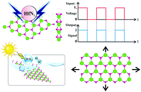
The response of the electronic properties of the HfN2 monolayer to external perturbation, such as strain and electric fields, has been extensively investigated using density functional theory calculations for its device-based applications and photocatalysis. The HfN2 monolayer is found to be a semiconductor showing a direct band gap of 1.44 eV, which is widely tunable by 0.9 eV via application of biaxial strain. Furthermore, the tunability in the band edges of the HfN2 monolayer straddling the water redox potential under a biaxial strain of ±10% makes it suitable for solar energy harvesting via photocatalytic applications over a wide range (0–7) of pH. The band gap can be decreased by 29.8% under a biaxial tensile strain of 10%. Upon incorporation of spin orbit coupling (SOC) a large spin splitting at the conduction band (Δc ∼ 314 meV) and a small splitting at the valence band (Δv ∼ 32 meV) are noted, which is attributable to the orbital composition of the band edges. The spin splitting in the band edges is found to be adjustable via biaxial compressive strain. The strain dependent mechanical properties and stability reveal the ability of the HfN2 monolayer to withstand a large magnitude of strain of up to ±10%, thereby bringing about a giant tunability in its Young modulus (Y) from 66 N m−1 to 283 N m−1, which is gainfully exploitable in flexible electronics. The tunability in Y over such a wide range has not been observed in other 2D materials. Moreover, the HfN2 monolayer undergoes a transition from a semiconducting to a metallic state under the application of a normal electric field or gate voltage of 0.48 V Å−1, which may potentially serve as the OFF (semiconducting) and ON (metallic) state in devices. Interestingly, an electric field of such intensity has been realized experimentally using pulsed ac field technology. Such a small gate voltage will greatly lower its power consumption. The electronic origin of this transition from the OFF to the ON state is found to arise from unoccupied NFEG (Nearly Free Electron Gas) states. A HfN2 monolayer based tunnel field effect transistor (t-FET) is proposed herewith as a model device for low-power digital data storage, thereby paving new avenues in flexible electronics and memory devices.
 Please wait while we load your content...

