Wet chemical growth of semiconductor 1-D nanostructure arrays on conductive substrates

Abstract
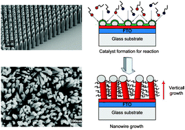
One-dimensional nanowire arrays directly grown on substrates have been recognized to be superior to two-dimensional thin films and nanoparticle films since they demonstrate in general single crystallinity, larger surface area, fast charge separation, and good contact with substrates. Accordingly, they provide an accessible way to the development of high performance devices such as photovoltaic cells, sensors, photocatalysts, electrodes, light emitters, etc. Although high-temperature vapor-phase synthesis is the most commonly employed method to produce high-crystallinity and high-density one-dimensional nanostructures with high purity, it is not acceptable in terms of the growing demand for the use of TCO (transparent conducting oxide) glass substrates, cost-effectiveness, and large scale mass production. Also, it is very difficult to control the precursor vapor pressures to meet the stoichiometry of many compound semiconductors through the vapor phase growth. In this context, there is a high need for the development of appropriate and efficient wet-chemical growth methods for one-dimensional nanostructures for a broad range of applications. In this review, we provide an overview of various low-temperature wet chemical synthetic approaches. In each fabrication method, we summarize the brief synthetic routes, microstructures, and the mechanism of anisotropic growth. In addition, the last section introduces various applications of one-dimensional nanostructure arrays. This review provides the current status and prospects of the growth of one-dimensional nanostructure arrays via wet chemical routes.
- This article is part of the themed collection: Recent Review Articles
 Please wait while we load your content...

