Fabrication of SnS nanowalls via pulsed plasma-enhanced chemical vapor deposition using a metal–organic single-source precursor†
 *a
Young Joo
Lee,
b
*a
Young Joo
Lee,
b
Abstract
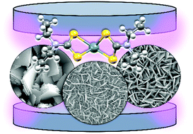
Orthorhombic tin(II)sulfide (α-SnS) is a IV–VI p-type semiconductor that is characterized by its layered crystal structure, resulting in a two-dimensional anisotropic crystal growth. The according interlayer gaps feature an enhanced electron mobility, compared to the charge mobility perpendicular to the growth direction. Consequently, when SnS is electrically contacted, light-generated charge carriers can be rapidly separated and transported along the interlayer gaps, so that charge-carrier recombination is minimized. This anisotropic electric transport might be utilized to improve the performance of optoelectronic devices, e.g., solar cells, when the absorbing layer consists of vertically aligned crystalline SnS nanowalls, following the vertical working geometry of the device. We report on the plasma-enhanced chemical vapor deposition (PECVD) of accurately aligned, highly crystalline SnS nanowalls on metal-covered wafer substrates. Our approach contains the thermal evaporation of a solid single-source precursor, mainly bis(diethyldithiocarbamato)tin(II), that is characterized in depth via, e.g., solid-state 119Sn-NMR spectroscopy. In situ optical emission spectroscopy of the plasma indicates the plasma-induced decomposition of the precursor. At an elevated substrate temperature of 400 °C, predominantly vertically oriented stacks of phase-pure SnS are grown, while at a low substrate temperature of 250 °C, very thin SnS nanowalls are formed, if the used wafer was covered with steel/18Cr/9Ni. Electric measurements of the SnS nanowalls indicate an enhanced conductivity in comparison to stacked SnS.
 Please wait while we load your content...

