Realizing low-voltage operating crystalline monolayer organic field-effect transistors with a low contact resistance†
Abstract
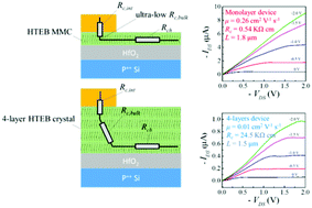
Enhancing charge injection from electrodes to the conducting channel and reducing the contact resistance (Rc) are valid strategies not only to improve the performance of organic field-effect transistors (OFETs), but also to enable low-voltage operating devices with a short channel. In order to improve the charge injection efficiency, many efforts have been made to reduce the interfacial injection resistance (Rc,int) in the past few decades, such as by adjusting the metal work function, inserting a buffer layer and so on. However, the method of decreasing the bulk injection resistance (Rc,bulk) in the vertical direction of the semiconductor layer is rarely studied. In this paper, two-dimensional (2D) monolayer and multilayer single-crystal devices of 1,4-bis((5′-hexyl-2,2′-bithiophen-5-yl)ethynyl)benzene (HTEB) were fabricated to study the dependence of the contact resistance of OFETs on crystal thickness. Devices based on monolayer molecular crystals (MMCs), and 4-layer and 15-layer single-crystal devices were found to have Rc of 1.77 kΩ cm, 26.9 kΩ cm and 5.15 MΩ cm, respectively. Thanks to the lower Rc, the MMC devices possess more steady linear mobility at a varied VDS, and a smaller deviation of the linear and saturation mobility. Finally, a low-voltage operating (−2 V) HTEB MMC device was fabricated on a 30 nm HfO2 insulating layer with an ultra-low Rc of 540 Ω cm.


 Please wait while we load your content...