Nanoscale depth control of implanted shallow silicon vacancies in silicon carbide†

Abstract
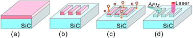
Color centers in silicon carbide have recently attracted broad interest as high bright single photon sources and defect spins with long coherence time at room temperature. There have been several methods to generate silicon vacancy defects with excellent spin properties in silicon carbide, such as electron irradiation and ion implantation. However, little is known about the depth distribution and nanoscale depth control of the shallow defects. Here, a method is presented to precisely control the depths of the ion implantation induced shallow silicon vacancy defects in silicon carbide by using reactive ion etching with little surface damage. After optimizing the major etching parameters, a slow and stable etching rate of about 5.5 ± 0.5 nm min−1 can be obtained. By successive nanoscale plasma etching, the shallow defects are brought close to the surface step by step. The photoluminescence spectrum and optically detected magnetic resonance spectra are measured, which confirm that there were no plasma-induced optical and spin property changes of the defects. By tracing the mean counts of the remaining defects after each etching process, the depth distribution of the defects can be obtained for various implantation conditions. Moreover, the spin coherence time T2* of the generated VSi defects is detected at different etch depths, which greatly decreases when the depth is less than 25 nm. The method of nanoscale depth control of silicon vacancies would pave the way for investigating the surface spin properties and the applications in nanoscale sensing and quantum photonics.
 Please wait while we load your content...

