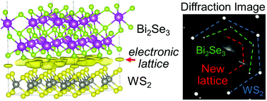
Evidence of a purely electronic two-dimensional lattice at the interface of TMD/Bi2Se3 heterostructures†
Abstract
When 2D materials are vertically stacked, new physics emerges from interlayer orbital interactions and charge transfer modulated by the additional periodicity of interlayer atomic registry (moiré superlattice). Surprisingly, relatively little is known regarding the real-space distribution of the transferred charges within this framework. Here we provide the first experimental indications of a real-space, non-atomic lattice formed by interlayer coupling induced charge redistribution in vertically stacked Bi2Se3/transition metal dichalcogenide (TMD) 2D heterostructures. Robust enough to scatter 200 keV electron beams, this non-atomic lattice generates selected area diffraction patterns that correspond excellently with simulated patterns from moiré superlattices of the parent crystals suggesting their location at sites of high interlayer atomic registry. Density functional theory (DFT) predicts concentrated charge pools reside in the interlayer region, located at sites of high nearest-neighbor atomic registry, suggesting the non-atomic lattices are standalone, reside in the interlayer region, and are purely electronic.


 Please wait while we load your content...