
Dose-dependent effect of proton irradiation on electrical properties of WSe2 ambipolar field effect transistors†

Abstract
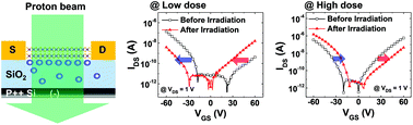
The irradiation effect of high energy proton beams on tungsten diselenide (WSe2) ambipolar field-effect transistors was investigated. We measured the electrical characteristics of the fabricated WSe2 FETs before and after the 10 MeV proton beam irradiation with different doses of 1012, 1013, 1014, and 1015 cm−2. For low dose conditions (1012, 1013, and 1014 cm−2), the threshold voltages shifted to the negative gate voltage direction, and the current in the hole and electron accumulation regimes decreased and increased, respectively. However, the trends were opposite for the high dose condition (1015 cm−2); the threshold voltages shifted to the positive gate voltage direction, and the current in the hole and electron accumulation regimes increased and decreased, respectively. These phenomena can be explained by the combined effect of proton irradiation-induced traps and the applied gate bias condition. Specifically, irradiation-induced positive oxide traps in SiO2 dielectrics play a role in enhancing electron accumulation and reducing hole accumulation in the WSe2 channel, whereas the irradiation-induced holes near the WSe2/SiO2 interface act as electron trapping sites, with enhancing hole accumulation and reducing electron accumulation in the WSe2 channel. This work will help improve the understanding of the effect of high energy irradiation on WSe2-based and other ambipolar nanoelectronic devices. In addition, this work shows the possibility of tuning the electrical properties of WSe2-based devices.
 Please wait while we load your content...

