Issue 17, 2019

WS2 monolayer-based light-emitting devices in a vertical p–n architecture

Abstract

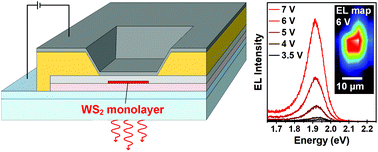
2D semiconductors represent an exciting new material class with great potential for optoelectronic devices. In particular, WS2 monolayers are promising candidates for light-emitting devices (LEDs) due to their direct band gap with efficient recombination in the red spectral range. Here, we present a novel LED architecture by embedding exfoliated WS2 monolayer flakes into a vertical p–n layout using organic p- and inorganic n-supporting layers. Laser lithography was applied to define the current path perpendicular to the WS2 flake. The devices exhibit rectifying behavior and emit room temperature electroluminescence with luminance up to 50 cd m−2 in the red spectral range.

Graphical abstract: WS2 monolayer-based light-emitting devices in a vertical p–n architecture

Supplementary files

Article information

Article type
Paper
Submitted
20 Feb 2019
Accepted
28 Mar 2019
First published
29 Mar 2019

Nanoscale, 2019,11, 8372-8379

WS2 monolayer-based light-emitting devices in a vertical p–n architecture

D. Andrzejewski, E. Hopmann, M. John, T. Kümmell and G. Bacher, Nanoscale, 2019, 11, 8372 DOI: 10.1039/C9NR01573F

To request permission to reproduce material from this article, please go to the Copyright Clearance Center request page.

If you are an author contributing to an RSC publication, you do not need to request permission provided correct acknowledgement is given.

If you are the author of this article, you do not need to request permission to reproduce figures and diagrams provided correct acknowledgement is given. If you want to reproduce the whole article in a third-party publication (excluding your thesis/dissertation for which permission is not required) please go to the Copyright Clearance Center request page.

Read more about how to correctly acknowledge RSC content.

Social activity

Spotlight

Advertisements